Deep-Dive with AI
Search across all available documentation for this part.

Deep-Dive with AI
Technical Specifications
Parameters and characteristics for this part
| Specification | AD7837AR-REEL |
|---|---|
| Architecture | R-2R |
| Data Interface | Parallel |
| Differential Output | False |
| INL/DNL (LSB) | ±1 (Max) |
| Mounting Type | Surface Mount |
| Number of Bits | 12 bits |
| Operating Temperature [Max] | 85 °C |
| Operating Temperature [Min] | -40 °C |
| Output Type | Voltage - Buffered |
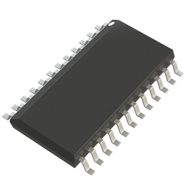
| Package / Case | 24-SOIC |
| Package / Case [custom] | 7.5 mm |
| Package / Case [custom] | 0.295 in |
| Reference Type | External |
| Settling Time | 5 µs |
| Supplier Device Package | 24-SOIC |
| Voltage - Supply, Analog [Max] | 15.75 V |
| Voltage - Supply, Analog [Min] | -14.25 V |
Pricing
Prices provided here are for design reference only. For realtime values and availability, please visit the distributors directly
| Distributor | Package | Quantity | $ | |
|---|---|---|---|---|
Description
General part information
AD7837 Series
The AD7837 /AD7847is a complete, dual, 12-bit multiplying digital-to-analog converter with output amplifiers on a monolithic CMOS chip. No external user trims are required to achieve full specified performance.Both parts are microprocessor compatible, with high speed data latches and interface logic. The AD7847 accepts 12-bit parallel data which is loaded into the respective DAC latch using theWRinput and a separate Chip Select input for each DAC. The AD7837 has a double-buffered 8-bit bus interface structure with data loaded to the respective input latch in two write operations. An asynchronousLDACsignal on the AD7837 updates the DAC latches and analog outputs.The output amplifiers are capable of developing ±10 V across a 2 kΩ load. They are internally compensated with low input offset voltage due to laser trimming at wafer level.The amplifier feedback resistors are internally connected to VOUTon the AD7847.The AD7837 / AD7847 is fabricated in Linear Compatible CMOS (LC2MOS), an advanced, mixed technology process that combines precision bipolar circuits with low power CMOS logic.A novel low leakage configuration (U.S. Patent No. 4,590,456) ensures low offset errors over the specified temperature range.
Documents
Technical documentation and resources


