Deep-Dive with AI
Search across all available documentation for this part.

Deep-Dive with AI
Technical Specifications
Parameters and characteristics for this part
| Specification | MCP1406T-E/MFVAO |
|---|---|
| Channel Type | Single |
| Current - Peak Output (Source, Sink) [custom] | 6 A |
| Current - Peak Output (Source, Sink) [custom] | 6 A |
| Driven Configuration | Low-Side |
| Gate Type | MOSFET (N-Channel, P-Channel), IGBT |
| Grade | Automotive |
| Input Type | Inverting |
| Mounting Type | Surface Mount |
| Number of Drivers | 1 |
| Operating Temperature [Max] | 125 °C |
| Operating Temperature [Min] | -40 °C |
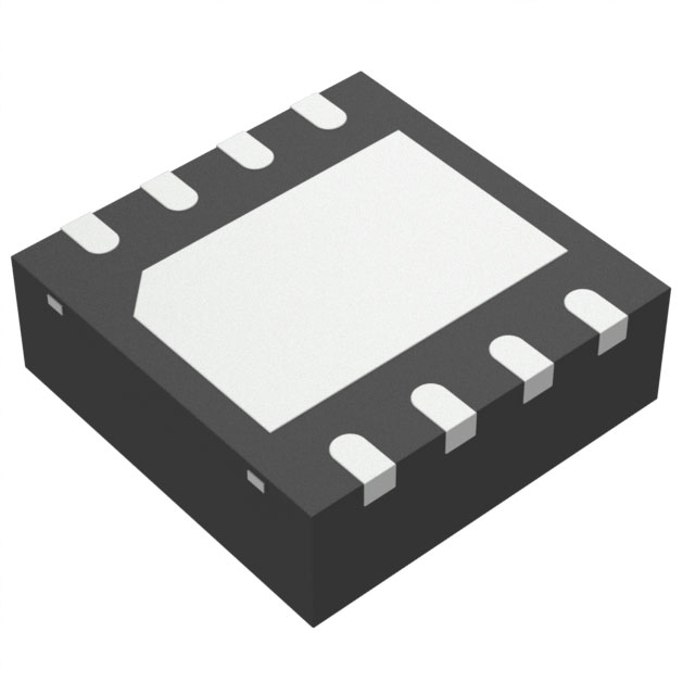
| Package / Case | 8-VDFN Exposed Pad |
| Qualification | AEC-Q100 |
| Rise / Fall Time (Typ) [custom] | 20 ns |
| Rise / Fall Time (Typ) [custom] | 20 ns |
| Supplier Device Package | 8-DFN-S (6x5) |
| Voltage - Supply [Max] | 18 V |
| Voltage - Supply [Min] | 4.5 V |
Pricing
Prices provided here are for design reference only. For realtime values and availability, please visit the distributors directly
| Distributor | Package | Quantity | $ | |
|---|---|---|---|---|
Description
General part information
MCP1406 Series
The MCP1406/07 devices are a family of buffers/MOSFET gate drivers that feature a single-output with 6 A peak drive current capability, low shoot-through current, matched rise/fall times and propagation delay times. These devices are pin-compatible and are improved versions of the TC4420/TC4429 MOSFET gate drivers.
The MCP1406/07 MOSFET gate drivers can easily charge and discharge 2500 pF gate capacitance in under 20 ns, provide low enough impedances (in both the ON and OFF states) to ensure that intended state of the MOSFETs will not be affected, even by large transients. The input to the MCP1406/07 may be driven directly from either TTL or CMOS (3 V to 18 V).
These devices are highly latch-up resistant under any conditions that fall within their power and voltage ratings. They are not subject to damage when up to 5 V of noise spiking (of either polarity) occurs on the ground pin. All terminals are fully protected against electrostatic discharge (ESD), up to 2.0 kV (HBM) and 400V (MM).
Documents
Technical documentation and resources


