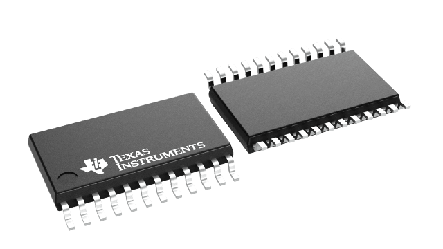
SN74LVTH543-EP Series
Enhanced Product 3.3-V Abt Octal Registered Transceivers With 3-State Outputs
Manufacturer: Texas Instruments
Catalog
Enhanced Product 3.3-V Abt Octal Registered Transceivers With 3-State Outputs
Key Features
• Controlled BaselineOne Assembly/Test Site, One Fabrication SiteEnhanced Diminishing Manufacturing Sources (DMS) SupportEnhanced Product-Change NotificationQualification PedigreeSupports Mixed-Mode Signal Operation (5-V Input and Output Voltages With 3.3-V VCC)Typical VOLP(Output Ground Bounce)<0.8 V at VCC= 3.3 V, TA= 25°CSupports Unregulated Battery Operation Down to 2.7 VIoffand Power-Up 3-State Support Hot InsertionBus Hold on Data Inputs Eliminates the Need for External Pullup/Pulldown ResistorsLatch-Up Performance Exceeds 500 mA Per JESD 17ESD Protection Exceeds JESD 222000-V Human-Body Model (A114-A)200-V Machine Model (A115-A)Component qualification in accordance with JEDEC and industry standards to ensure reliable operation over an extended temperature range. This includes, but is not limited to, Highly Accelerated Stress Test (HAST) or biased 85/85, temperature cycle, autoclave or unbiased HAST, electromigration, bond intermetallic life, and mold compound life. Such qualification testing should not be viewed as justifying use of this component beyond specified performance and environmental limits.Controlled BaselineOne Assembly/Test Site, One Fabrication SiteEnhanced Diminishing Manufacturing Sources (DMS) SupportEnhanced Product-Change NotificationQualification PedigreeSupports Mixed-Mode Signal Operation (5-V Input and Output Voltages With 3.3-V VCC)Typical VOLP(Output Ground Bounce)<0.8 V at VCC= 3.3 V, TA= 25°CSupports Unregulated Battery Operation Down to 2.7 VIoffand Power-Up 3-State Support Hot InsertionBus Hold on Data Inputs Eliminates the Need for External Pullup/Pulldown ResistorsLatch-Up Performance Exceeds 500 mA Per JESD 17ESD Protection Exceeds JESD 222000-V Human-Body Model (A114-A)200-V Machine Model (A115-A)Component qualification in accordance with JEDEC and industry standards to ensure reliable operation over an extended temperature range. This includes, but is not limited to, Highly Accelerated Stress Test (HAST) or biased 85/85, temperature cycle, autoclave or unbiased HAST, electromigration, bond intermetallic life, and mold compound life. Such qualification testing should not be viewed as justifying use of this component beyond specified performance and environmental limits.
Description
AI
These octal transceivers are designed specifically for low-voltage (3.3-V) VCCoperation, but with the capability to provide a TTL interface to a 5-V system environment.
The ’LVTH543 devices contain two sets of D-type latches for temporary storage of data flowing in either direction. Separate latch-enable (LEAB\ or LEBA\) and output-enable (OEAB\ or OEBA\) inputs are provided for each register, to permit independent control in either direction of data flow.
The A-to-B enable (CEAB)\ input must be low to enter data from A or to output data from B. If CEAB\ is low and LEAB\ is low, the A-to-B latches are transparent; a subsequent low-to-high transition of LEAB\ puts the A latches in the storage mode. With CEAB\ and OEAB\ both low, the 3-state B outputs are active and reflect the data present at the output of the A latches. Data flow from B to A is similar, but requires using the CEBA\, LEBA\, and OEBA\ inputs.
Active bus-hold circuitry holds unused or undriven inputs at a valid logic state. Use of pullup or pulldown resistors with the bus-hold circuitry is not recommended.
When VCCis between 0 and 1.5 V, the device is in the high-impedance state during power up or power down. However, to ensure the high-impedance state above 1.5 V, OE\ should be tied to VCCthrough a pullup resistor; the minimum value of the resistor is determined by the current-sinking capability of the driver.
This device is fully specified for hot-insertion applications using Ioffand power-up 3-state. The Ioffcircuitry disables the outputs, preventing damaging current backflow through the device when it is powered down. The power-up 3-state circuitry places the outputs in the high-impedance state during power up and power down, which prevents driver conflict.


