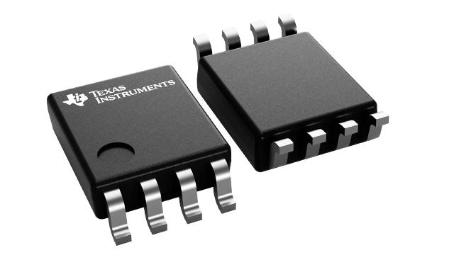
SN74LVC2G126-EP Series
Enhanced product 2-ch, 1.65-V to 5.5-V buffers with 3-state outputs
Manufacturer: Texas Instruments
Catalog
Enhanced product 2-ch, 1.65-V to 5.5-V buffers with 3-state outputs
Key Features
• Supports 5-V VCCOperationInputs Accept Voltages to 5.5 VMax tpdof 6.8 ns at 3.3 VLow Power Consumption, 10-μA Max ICC±24-mA Output Drive at 3.3 VTypical VOLP(Output Ground Bounce)<0.8 V at VCC= 3.3 V, TA= 25°CTypical VOHV(Output VOHUndershoot)>2 V at VCC= 3.3 V, TA= 25°CIoffSupports Partial-Power-Down Mode OperationLatch-Up Performance Exceeds 100 mA Per JESD 78, Class IIESD Protection Exceeds JESD 222000-V Human-Body Model (A114-A)200-V Machine Model (A115-A)1000-V Charged-Device Model (C101)SUPPORTS DEFENSE, AEROSPACE, AND MEDICAL APPLICATIONSControlled BaselineOne Assembly and Test SiteOne Fabrication SiteAvailable in Military (–55°C to 125°C) Temperature RangeExtended Product Life CycleExtended Product-Change NotificationProduct TraceabilitySupports 5-V VCCOperationInputs Accept Voltages to 5.5 VMax tpdof 6.8 ns at 3.3 VLow Power Consumption, 10-μA Max ICC±24-mA Output Drive at 3.3 VTypical VOLP(Output Ground Bounce)<0.8 V at VCC= 3.3 V, TA= 25°CTypical VOHV(Output VOHUndershoot)>2 V at VCC= 3.3 V, TA= 25°CIoffSupports Partial-Power-Down Mode OperationLatch-Up Performance Exceeds 100 mA Per JESD 78, Class IIESD Protection Exceeds JESD 222000-V Human-Body Model (A114-A)200-V Machine Model (A115-A)1000-V Charged-Device Model (C101)SUPPORTS DEFENSE, AEROSPACE, AND MEDICAL APPLICATIONSControlled BaselineOne Assembly and Test SiteOne Fabrication SiteAvailable in Military (–55°C to 125°C) Temperature RangeExtended Product Life CycleExtended Product-Change NotificationProduct Traceability
Description
AI
This dual bus buffer gate is designed for 1.65-V to 5.5-V VCCoperation.
The SN74LVC2G126 is a dual bus driver/line driver with 3-state outputs. The outputs are disabled when the associated output-enable (OE) input is low.
To ensure the high-impedance state during power up or power down, OE should be tied to GND through a pulldown resistor; the minimum value of the resistor is determined by the current-sourcing capability of the driver.
This device is fully specified for partial-power-down applications using Ioff. The Ioffcircuitry disables the outputs, preventing damaging current backflow through the device when it is powered down.


