SN74CB3Q3305 Series
3.3-V, 1:1 (SPST), 2-channel FET bus switch (active high)
Manufacturer: Texas Instruments
Catalog
3.3-V, 1:1 (SPST), 2-channel FET bus switch (active high)
Key Features
• High-bandwidth data path (up to 500 MHz)(1)5-V tolerant I/Os with device powered up or powered downLow and flat ON-state resistance (ron) characteristics over operating range (ron= 3 Ω typical)Supports input voltage beyond supply on data I/O ports0 to 5 V switching with 3.3 V VCC0 to 3.3 V switching with 2.5 V VCCBidirectional data flow with near-zero propagation delayLow input or output capacitance minimizes loading and signal distortion (Cio(OFF)= 3.5 pF typical)Fast switching frequency (fOE= 20 MHz maximum)Data and control inputs provide undershoot clamp diodesLow power consumption (ICC= 0.25 mA typical)VCCoperating range from 2.3 V to 3.6 VData I/Os support 0 to 5 V signaling levels (0.8 V, 1.2 V, 1.5 V, 1.8 V, 2.5 V, 3.3 V, and 5 V)Control inputs can be driven by TTL or 5 V/3.3 V CMOS outputsIoffsupports partial-power-down mode operationLatch-up performance exceeds 100 mA per JESD 78, Class II(1)For additional information regarding the performance characteristics of the CB3Q family, refer to the TI application report,CBT-C, CB3T, and CB3Q Signal-Switch Families,SCDA008.High-bandwidth data path (up to 500 MHz)(1)5-V tolerant I/Os with device powered up or powered downLow and flat ON-state resistance (ron) characteristics over operating range (ron= 3 Ω typical)Supports input voltage beyond supply on data I/O ports0 to 5 V switching with 3.3 V VCC0 to 3.3 V switching with 2.5 V VCCBidirectional data flow with near-zero propagation delayLow input or output capacitance minimizes loading and signal distortion (Cio(OFF)= 3.5 pF typical)Fast switching frequency (fOE= 20 MHz maximum)Data and control inputs provide undershoot clamp diodesLow power consumption (ICC= 0.25 mA typical)VCCoperating range from 2.3 V to 3.6 VData I/Os support 0 to 5 V signaling levels (0.8 V, 1.2 V, 1.5 V, 1.8 V, 2.5 V, 3.3 V, and 5 V)Control inputs can be driven by TTL or 5 V/3.3 V CMOS outputsIoffsupports partial-power-down mode operationLatch-up performance exceeds 100 mA per JESD 78, Class II(1)For additional information regarding the performance characteristics of the CB3Q family, refer to the TI application report,CBT-C, CB3T, and CB3Q Signal-Switch Families,SCDA008.
Description
AI
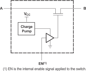
The SN74CB3Q3305 device is a high-bandwidth FET bus switch using a charge pump to elevate the gate voltage of the pass transistor, providing a low and flat ON-state resistance (ron). The low and flat ON-state resistance allows for minimal propagation delay and supports switching input voltage beyond the supply on the data input/output (I/O) ports. The device also features low data I/O capacitance to minimize capacitive loading and signal distortion on the data bus. Specifically designed to support high-bandwidth applications, the SN74CB3Q3305 device provides an optimized interface solution ideally suited for broadband communications, networking, and data-intensive computing systems.
This device is fully specified for partial-power-down applications using Ioff. The Ioffcircuitry prevents damaging current backflow through the device when it is powered down. The device has isolation during power off.
To ensure the high-impedance state during power up or power down, OE should be tied to GND through a pulldown resistor; the minimum value of the resistor is determined by the current-sourcing capability of the driver.


