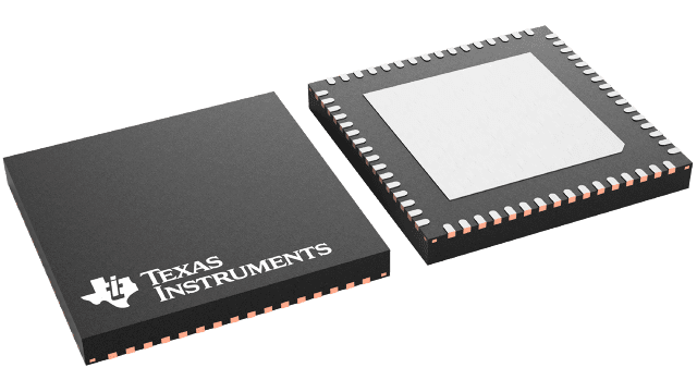
LMK5C33216AS1 Series
Three DPLL, three APLL, two-input and 16-output network synchronizer with BAW VCO IEEE-1588 support
Manufacturer: Texas Instruments
Catalog
Three DPLL, three APLL, two-input and 16-output network synchronizer with BAW VCO IEEE-1588 support
Key Features
• Ultra-low jitter BAW VCO based Wireless clocks40fs typical/ 57fs maximum RMS jitter at 491.52MHz50fs typical/ 62fs maximum RMS jitter at 245.76MHzThree high-performance Digital Phase Locked Loops (DPLLs) with paired Analog Phase Locked Loops (APLLs)Programmable DPLL loop bandwidth from 1mHz to 4kHz< 1ppt DCO frequency adjustment step sizeTwo differential or single-ended DPLL inputs1Hz (1PPS) to 800MHz input frequencyDigital holdover and hitless switching16 differential outputs with programmable HSDS, AC-LVPECL, LVDS, and HSCL formatsUp to 20 total frequency outputs when configured with 6 LVCMOS frequency outputs on OUT[1:0]_P/N, GPIO1, and GPIO2 and 14 differential outputs on OUT[15:0]_P/N1Hz (1PPS) to 1250MHz output frequency with programmable swing and common modePCIe Gen 1 to 6 compliantI2C, 3-wire SPI, or 4-wire SPI–40°C to 85°C operating temperatureUltra-low jitter BAW VCO based Wireless clocks40fs typical/ 57fs maximum RMS jitter at 491.52MHz50fs typical/ 62fs maximum RMS jitter at 245.76MHzThree high-performance Digital Phase Locked Loops (DPLLs) with paired Analog Phase Locked Loops (APLLs)Programmable DPLL loop bandwidth from 1mHz to 4kHz< 1ppt DCO frequency adjustment step sizeTwo differential or single-ended DPLL inputs1Hz (1PPS) to 800MHz input frequencyDigital holdover and hitless switching16 differential outputs with programmable HSDS, AC-LVPECL, LVDS, and HSCL formatsUp to 20 total frequency outputs when configured with 6 LVCMOS frequency outputs on OUT[1:0]_P/N, GPIO1, and GPIO2 and 14 differential outputs on OUT[15:0]_P/N1Hz (1PPS) to 1250MHz output frequency with programmable swing and common modePCIe Gen 1 to 6 compliantI2C, 3-wire SPI, or 4-wire SPI–40°C to 85°C operating temperature
Description
AI
The LMK5C33216AS1 is a high-performance network synchronizer and jitter cleaner designed to meet the stringent requirements of wireless communications and infrastructure applications.
The device is bundled with software support for IEEE-1588 PTP synchronization to a primary reference clock source. For more information, contact TI.
The device integrates three DPLLs and three APLLs to provide hitless switching and jitter attenuation with programmable loop bandwidth (LBW) and one external loop filter capacitor, maximizing flexibility and ease of use.
APLL3 features an ultra-high performance PLL with TI’s proprietary Bulk Acoustic Wave (BAW) technology. The BAW APLL can generate 491.52MHz output clocks with 40fs typical / 60fs maximum RMS jitter (12kHz to 20MHz) irrespective of the DPLL reference input frequency and jitter characteristics. APLL2 and APLL1 (conventional LC VCOs) provide options for a second or third frequency and/or synchronization domain.
Reference validation circuitry monitors the DPLL reference inputs and automatically performs a hitless switch when the inputs are detected or lost. Zero-Delay Mode (ZDM) provides control over the phase relationship between inputs and outputs.
The device is fully programmable through I2C or SPI. The integrated EEPROM can be used to customize system start-up clocks. The device also features factory default ROM profiles as fallback options.


