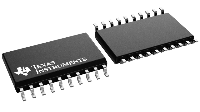
CLVC574 Series
Automotive Catalog Octal Edge-Triggered D-Type Flip-Flop With 3-State Outputs
Manufacturer: Texas Instruments
Catalog
Automotive Catalog Octal Edge-Triggered D-Type Flip-Flop With 3-State Outputs
Key Features
• Qualified for Automotive ApplicationsESD Protection Exceeds 2000 V PerMIL-STD-883, Method 3015; Exceeds 200 V Using Machine Model (C = 200 pF, R = 0)Operates From 2 V to 3.6 VInputs Accept Voltages to 5.5 VMax tpdof 7 ns at 3.3 VTypical VOLP(Output Ground Bounce) < 0.8 V at VCC= 3.3 V, TA= 25°CTypical VOHV(Output VOHUndershoot) > 2 V at VCC= 3.3 V, TA= 25°CSupports Mixed-Mode Signal Operation on All Ports (5-V Input/Output Voltage With 3.3-V VCC)IoffSupports Partial-Power-Down Mode OperationQualified for Automotive ApplicationsESD Protection Exceeds 2000 V PerMIL-STD-883, Method 3015; Exceeds 200 V Using Machine Model (C = 200 pF, R = 0)Operates From 2 V to 3.6 VInputs Accept Voltages to 5.5 VMax tpdof 7 ns at 3.3 VTypical VOLP(Output Ground Bounce) < 0.8 V at VCC= 3.3 V, TA= 25°CTypical VOHV(Output VOHUndershoot) > 2 V at VCC= 3.3 V, TA= 25°CSupports Mixed-Mode Signal Operation on All Ports (5-V Input/Output Voltage With 3.3-V VCC)IoffSupports Partial-Power-Down Mode Operation
Description
AI
The SN74LVC574A octal edge-triggered D-type flip-flop is designed for 2.7-V to 3.6-V VCCoperation.
This device features 3-state outputs designed specifically for driving highly capacitive or relatively low-impedance loads. It is particularly suitable for implementing buffer registers, I/O ports, bidirectional bus drivers, and working registers.
On the positive transition of the clock (CLK) input, the Q outputs are set to the logic levels at the data (D) inputs.
A buffered output-enable (OE) input can be used to place the eight outputs in either a normal logic state (high or low logic levels) or the high-impedance state. In the high-impedance state, the outputs neither load nor drive the bus lines significantly. The high-impedance state and increased drive provide the capability to drive bus lines without interface or pullup components.
OEdoes not affect the internal operations of the flip-flops. Old data can be retained or new data can be entered while the outputs are in the high-impedance state.
This device is fully specified for partial-power-down applications using Ioff. The Ioffcircuitry disables the outputs, preventing damaging current backflow through the device when it is powered down.
To ensure the high-impedance state during power up or power down,OEshould be tied to VCCthrough a pullup resistor; the minimum value of the resistor is determined by the current-sinking capability of the driver.
Inputs can be driven from either 3.3-V or 5-V devices. This feature allows the use of thIs device as a translator in a mixed 3.3-V/5-V system environment.


