AD5542A Series
2.7 V to 5.5 V, Serial-Input, Voltage-Output, 16-BitnanoDAC™in 10-lead LFCSP, 16-lead 3 mm x 3 mm LFCSP, and 16-lead TSSOP
Manufacturer: Analog Devices
Catalog
2.7 V to 5.5 V, Serial-Input, Voltage-Output, 16-BitnanoDAC™in 10-lead LFCSP, 16-lead 3 mm x 3 mm LFCSP, and 16-lead TSSOP
Key Features
• Full 16-bit performance
• 3 V and 5 V single-supply operation
• Low 0.625 mW power dissipation
• 1 μs settling time
• Unbuffered voltage output capable of driving 60 kΩ loads directly
• SPI-/QSPI-/MICROWIRE-compatible interface standards
• Power-on reset clears DAC output to 0 V (unipolar mode)
• 5 kV HBM ESD classification
• Low glitch: 1.1 nV-sec
Description
AI
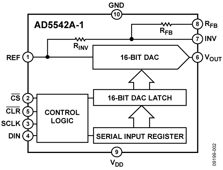
TheAD5541/ AD5542 are single, 16-bit, serial input, voltage output digital-to-analog converters (DACs) that operate from a single 2.7 V to 5.5 V supply. The DAC output range extends from 0 V to VREF.The DAC output range extends from 0 V to VREFand is guaranteed monotonic, providing 1 LSB INL accuracy at 16 bits without adjustment over the full specified temperature range of −40°C to +85°C. Offering unbuffered outputs, the AD5541 / AD5542 achieve a 1 μs settling time with low power consumption and low offset errors. Providing a low noise performance of 11.8 nV/√Hzand low glitch, the AD5541 / AD5542 is suitable for deployment across multiple end systems.The AD5542 can be operated in bipolar mode, which generates a ±VREFoutput swing. The AD5542 also includes Kelvin sense connections for the reference and analog ground pins to reduce layout sensitivity.The AD5541 / AD5542 utilize a versatile 3-wire interface that is compatible with SPI, QSPI™, MICROWIRE™, and DSP interface standards. The AD5541 / AD5542 are available in 8-lead and 14-lead SOIC packages.PRODUCT HIGHLIGHTSSingle-Supply Operation. The AD5541 and AD5542 are fully specified and guaranteed for a single 2.7 V to 5.5 V supply.Low Power Consumption. These parts consume typically 0.625 mW with a 5 V supply and 0.375 mW at 3 V.3-Wire Serial Interface.Unbuffered Output Capable of Driving 60 kΩ Loads. This reduces power consumption because there is no internal buffer to drive.Power-On Reset Circuitry.APPLICATIONSDigital gain and offset adjustmentAutomatic test equipmentData acquisition systemsIndustrial process control


