SN74LV541AT Series
8-ch, 4.5-V to 5.5-V buffers with TTL-compatible CMOS inputs and 3-state outputs
Manufacturer: Texas Instruments
Catalog
8-ch, 4.5-V to 5.5-V buffers with TTL-compatible CMOS inputs and 3-state outputs
Key Features
• Inputs Are TTL-Voltage Compatible4.5-V to 5.5-V VCCOperationTypical tpdof 4 ns at 5 VTypical VOLP(Output Ground Bounce)<0.8 V at VCC= 5 V, TA= 25°CTypical VOHV(Output VOHUndershoot)>2.3 V at VCC= 5 V, TA= 25°CSupports Mixed-Mode Voltage Operation on All PortsIoffSupports Partial-Power-Down Mode OperationLatch-Up Performance Exceeds 250 mA Per JESD 17ESD Protection Exceeds JESD 222000-V Human-Body Model (A114-A)200-V Machine Model (A115-A)1000-V Charged-Device Model (C101)Inputs Are TTL-Voltage Compatible4.5-V to 5.5-V VCCOperationTypical tpdof 4 ns at 5 VTypical VOLP(Output Ground Bounce)<0.8 V at VCC= 5 V, TA= 25°CTypical VOHV(Output VOHUndershoot)>2.3 V at VCC= 5 V, TA= 25°CSupports Mixed-Mode Voltage Operation on All PortsIoffSupports Partial-Power-Down Mode OperationLatch-Up Performance Exceeds 250 mA Per JESD 17ESD Protection Exceeds JESD 222000-V Human-Body Model (A114-A)200-V Machine Model (A115-A)1000-V Charged-Device Model (C101)
Description
AI
The SN74LV541AT is designed for 4.5-V to 5.5-V VCCoperation. The inputs are TTL-voltage compatible, which allows them to be interfaced with bipolar outputs and 3.3-V devices. The device also can be used to translate from 3.3 V to 5 V.
This device is ideal for driving bus lines or buffer memory address registers. It features inputs and outputs on opposite sides of the package to facilitate printed circuit board layout.
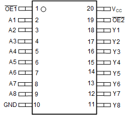
The 3-state control gate is a two-input AND gate with active-low inputs so that, if either output-enable (OE1orOE2) input is high, all corresponding outputs are in the high-impedance state. The outputs provide noninverted data when they are not in the high-impedance state.
To ensure the high-impedance state during power up or power down,OEshall be tied to VCC through a pullup resistor; the minimum value of the resistor is determined by the current-sinking capability of the driver.
This device is fully specified for partial-power-down applications using Ioff. The Ioffcircuitry disables the outputs, preventing damaging current backflow through the device when it is powered down.


