Catalog
16-bit, 33 MIPS, 5v, 2 Serial Ports, Host Port
Key Features
• 30 ns Instruction Cycle Time (33 MIPS) from 16.67 MHz Crystal at 5.0 V
• 50 ns Instruction Cycle Time (20 MIPS) from 10 MHz Crystal at 3.3 V
• ADSP-2100 Family Code & Function Compatible with New Instruction Set Enhancements for Bit Manipulation Instructions, Multiplication Instructions, Biased Rounding, and Global Interrupt Masking
• Bus Grant Hang Logic
• 2K Words of On-Chip Program Memory RAM
• 2K Words of On-Chip Data Memory RAM
• 8K Words of On-Chip Program Memory ROM (ADSP-2172)
• 8- or 16-Bit Parallel Host Interface Port
• 300 mW Typical Power Dissipation at 5.0 V at 30 ns
• 70 mW Typical Power Dissipation at 3.3 V at 50 ns
Description
AI
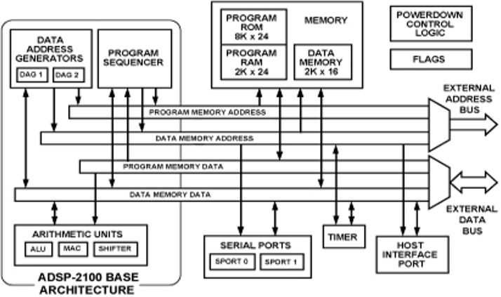
The ADSP-2171, ADSP-2172, and ADSP-2173 are single-chip microcomputers optimized for digital signal processing (DSP) and other high-speed numeric processing applications. The ADSP-2171 and ADSP-2172 are designed for 5.0 V applications. The ADSP-2173 is designed for 3.3 V applications. The ADSP-2172 also has 8K words (24-bit) of program ROM.The ADSP-217x combines the ADSP-2100 base architecture (three computational units, data address generators, and a program sequencer) with two serial ports, a host interface port, a programmable timer, extensive interrupt capabilities, and on-chip program and data memory.The ADSP-2171, ADSP-2172, and ADSP-2173 are single-chip microcomputers optimized for digital signal processing (DSP) and other high-speed numeric processing applications. The ADSP-2171 and ADSP-2172 are designed for 5.0 V applications. The ADSP-2173 is designed for 3.3 V applications. The ADSP-2172 also has 8K words (24-bit) of program ROM.The ADSP-217x combines the ADSP-2100 base architecture (three computational units, data address generators, and a program sequencer) with two serial ports, a host interface port, a programmable timer, extensive interrupt capabilities, and on-chip program and data memory.In addition, the ADSP-217x supports new instructions, which include bit manipulations-bit set, bit clear, bit toggle, bit test- new ALU constants, new multiplication instruction (x squared), biased rounding, and global interrupt masking, for increased flexibility. The ADSP-217x also has a Bus Grant Hang Logic (BGH) feature.The ADSP-217x provides 2K words (24-bit) of program RAM and 2K words (16-bit) of data memory. The ADSP-2172 provides an additional 8K words (24-bit) of program ROM. Power-down circuitry is also provided to meet the low power needs of battery operated portable equipment. The ADSP-217x is available in 128-pin TQFP and 128-pin PQFP packages.Fabricated in a high-speed, double metal, low power, CMOS process, the ADSP-217X operates with a 30 ns instruction cycle time. Every instruction can execute in a single processor cycle.The ADSP-217x's flexible architecture and comprehensive instruction set allow the processor to perform multiple operations in parallel. In one processor cycle the ADSP-217x can:generate the next program addressfetch the next instructionperform one or two data movesupdate one or two data address pointersperform a computational operationThis takes place while the processor continues to:receive and transmit data through the two serial portsreceive and/or transmit data through the host interface portdecrement timer


