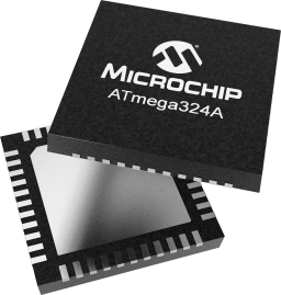
Catalog
Key Features
• * 131 Powerful Instructions
• * Most Single Clock Cycle Execution
• * 32 x 8 General Purpose Working Registers
• * Fully Static Operation
• * Up to 20 MIPS Throughput at 20 MHz
• * On-Chip Two-Cycle Multiplier
• * 32 KB of In-System Self-Programmable Flash program memory
• * 1 KB EEPROM
• * 2 KB Internal SRAM
• * Write/Erase Cycles: 10,000 Flash/100,000 EEPROM
• * Data retention: 20 years at 85°C
• * In-System Programming by On-chip Boot Program
• * True Read-While-Write Operation
• * Programming Lock for Software Security
• * Capacitive Touch Buttons, Sliders and Wheels
• * 24 Self-Cap Channels and 144 Mutual Cap Channels
• * Two 8-bit Timer/Counters with Separate Prescaler and Compare Mode
• * Three 16-bit Timer/Counters with Separate Prescaler, Compare Mode, and Capture Mode
• * Real Time Counter with Separate Oscillator
• * Ten PWM Channels
• * 8-channel 10-bit ADC in TQFP and QFN/MLF package
• * ThreeProgrammable Serial USARTs
• * Two Master/Slave SPI Serial Interfaces
• * Two Byte-Oriented Two-Wire Serial Interfaces (Philips I2C Compatible)
• * Programmable Watchdog Timer with Separate On-chip Oscillator
• * On-Chip Analog Comparator
• * Interrupt and Wake-Up on Pin Change
• * Power-On Reset and Programmable Brown-Out Detection
• * Internal 8 MHz Calibrated Oscillator
• * External and Internal Interrupt Sources
• * Six Sleep Modes: Idle, ADC Noise Reduction, Power-save, Power-down, Standby, and Extended Standby
• * Clock Failure Detection Mechanism and Switch to Internal 8 MHz RC Oscillator in case of Failure
• * Individual Serial Number to Represent a Unique ID
• * 39 Programmable I/O Lines
• * 44-pin TQFP and 44-pin QFN/MLF
• * 1.8-5.5V
• * -40°C to 105°C
• * 0-4 MHz @ 1.8 - 5.5V
• * 0-10 MHz @ 2.7 - 5.5.V
• * 0-20 MHz @ 4.5 - 5.5V
• * Active Mode: 0.24 mA
• * Power-Down Mode: 0.2 µA
• * Power-Save Mode: 1.3 µA (Including 32 kHz RTC)
Description
AI
The high-performance Microchip 8-bit AVR® RISC-based
picoPower® microcontroller combines 32 KB ISP Flash memory with read-while-write
capabilities, 1 KB EEPROM, 2 KB SRAM, 39 general purpose I/O lines, 32
general purpose working registers, five flexible timer/counters with
compare modes, internal and external interrupts, three USARTs with
wake-up on start of transmission, two byte-oriented Two-Wire serial
interface, two SPI serial ports, one 8-channel 10-bit ADC with optional
differential input stage with programmable gain, programmable watchdog
timer with internal oscillator, a JTAG (IEEE® 1149.1 compliant) test
interface for on-chip debugging and programming, and six software
selectable power saving modes. The device operates between 1.8-5.5
volts.
The ATmega324PB features the successful QTouch® Peripheral
Touch Controller (PTC). The PTC acquires signals to detect
touch on capacitive sensors and supports both self- and
mutual-capacitance sensors. The ATmega324PB PTC is supported by the
Microchip QTouch Composer development tool (QTouch Library project
builder and QTouch Analyzer). It provides a faster and less complex
capacitive touch implementation in any application.
The ATmega324PB supports 32
buttons in self-capacitance mode or up to 256 buttons in
mutual-capacitance mode. Mix-and-match mutual-and self-capacitance
sensors are possible. Only one pin is required per electrode, and no
external components are required, delivering savings on the BOM cost
compared to competing solutions.
By executing powerful
instructions in a single clock cycle, the device achieves throughputs
approaching one MIPS per MHz, balancing power consumption and processing
speed.


