Catalog
12-Bit, 170/210 MSPS 3.3 V A/D Converter
Key Features
• SNR = 65 dB @ fINup to 70 MHz @ 210 MSPS
• ENOB of 10.6 @ fINup to 70 MHz @ 210 MSPS
• Excellent Linearity:DNL = ±0.3 LSB (Typical)INL = ±0.5 LSB (Typical)
• Two Output Data Options:Demultiplexed 3.3 V CMOS Outputs Each @ 105 MSPSInterleaved or Parallel Data Output OptionLVDS at 210 MSPS
• SFDR = 80 dBc @ fINup to 70 MHz @ 210 MSPS
• 700 MHz Full Power Analog Bandwidth
• Power Dissipation = 1.3 W Typical @ 210 MSPS
• 1.5 V Input Voltage Range
• 3.3 V Supply Operation
• Output Data Format Option
• Data Sync Input and Data Clock Output Provided
• Clock Duty Cycle Stabilizer
Description
AI
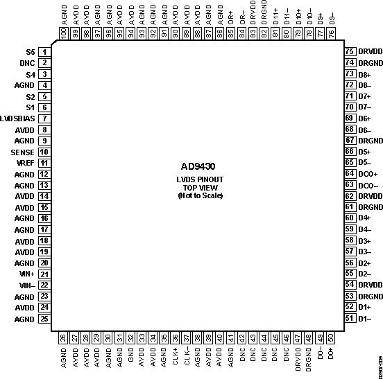
The AD9430 is a 12-bit monolithic sampling analog-to-digital converter optimized for high performance, low power, and ease of use. The product operates up to a 210 MSPS conversion rate and is optimized for outstanding dynamic performance in wideband carrier and broadband systems. All necessary functions, including a track-and-hold (T/H) and reference are included on the chip to provide a complete conversion solution.The ADC requires a 3.3 V power supply and a differential ENCODE clock for full performance operation. The digital outputs are TTL/CMOS or LVDS compatible and support either twos complement or offset binary format. Separate output power supply pins support interfacing with 3.3 V or 2.5 V CMOS logic.Two output buses support demultiplexed data up to 105 MSPS rates in CMOS mode. A data sync input is supported for proper output data port alignment in CMOS mode and a data clock output is available for proper output data timing. In LVDS mode, the chip provides data at the ENCODE clock rate.Fabricated on an advanced BiCMOS process, the AD9430 is available in a 100-lead surface-mount plastic package (100 e-PAD TQFP) specified over the industrial temperature range (-40°C to +85°C).APPLICATIONSWireless and Wired Broadband CommunicationsCable Reverse PathCommunications Test EquipmentRadar and Satellite SubsystemsPower Amplifier LinearizationPRODUCT HIGHLIGHTSHigh performance. Maintains 65 dB SNR @ 210 MSPS with a 65 MHz input.Low power. Consumes only 1.3 W @ 210 MSPS.Ease of use. LVDS output data and output clock signal allow interface to current FPGA technology. The on-chip reference and sample-and-hold provide flexibility in system design. Use of a single 3.3 V supply simplifies system power supply design.Out of range (OR) feature. The OR output bit indicates when the input signal is beyond the selected input range.Pin compatible with 10-bit AD9411 (LVDS only).


