CSD97370Q5M Series
30 V 25 A SON 5 x 6 mm synchronous buck NexFET™ power stage
Manufacturer: Texas Instruments
Catalog
30 V 25 A SON 5 x 6 mm synchronous buck NexFET™ power stage
Key Features
• 90% System Efficiency at 25AInput Voltages up to 22VHigh Frequency Operation (Up To 2MHz)Incorporates Power Block TechnologyHigh Density – SON 5-mm × 6-mm FootprintLow Power Loss 2.8W at 25AUltra Low Inductance PackageSystem Optimized PCB Footprint3.3V and 5V PWM Signal Compatible3-State PWM InputIntegrated Bootstrap DiodePre-Bias Start-Up ProtectionShoot Through ProtectionRoHS Compliant – Lead Free Terminal Plating Halogen Free90% System Efficiency at 25AInput Voltages up to 22VHigh Frequency Operation (Up To 2MHz)Incorporates Power Block TechnologyHigh Density – SON 5-mm × 6-mm FootprintLow Power Loss 2.8W at 25AUltra Low Inductance PackageSystem Optimized PCB Footprint3.3V and 5V PWM Signal Compatible3-State PWM InputIntegrated Bootstrap DiodePre-Bias Start-Up ProtectionShoot Through ProtectionRoHS Compliant – Lead Free Terminal Plating Halogen Free
Description
AI
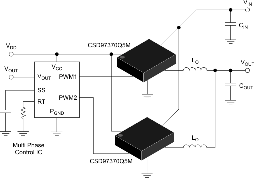
The CSD97370Q5M NexFET Power Stage is an optimized design for use in a high power, high density Synchronous Buck converter. This product integrates an enhanced gate driver IC and Power Block Technology to complete the power stage switching function. This combination produces a high current, high efficiency, high speed switching device and delivers an excellent thermal solution in a small 5-mm × 6-mm outline package due to its large ground based thermal pad. In addition, the PCB footprint has been optimized to help reduce design time and simplify the completion of the overall system design.
The CSD97370Q5M NexFET Power Stage is an optimized design for use in a high power, high density Synchronous Buck converter. This product integrates an enhanced gate driver IC and Power Block Technology to complete the power stage switching function. This combination produces a high current, high efficiency, high speed switching device and delivers an excellent thermal solution in a small 5-mm × 6-mm outline package due to its large ground based thermal pad. In addition, the PCB footprint has been optimized to help reduce design time and simplify the completion of the overall system design.


