TPS22932B Series
3.6-V, 0.5-A, 55-mΩ, 80nA leakage load switch with output discharge
Manufacturer: Texas Instruments
Catalog
3.6-V, 0.5-A, 55-mΩ, 80nA leakage load switch with output discharge
Key Features
• Input Voltage: 1.1 V to 3.6 VUltralow ON-ResistancerON= 55 mΩ at VIN= 3.6 VrON= 65 mΩ at VIN= 2.5 VrON= 75 mΩ at VIN= 1.8 VrON= 115 mΩ at VIN= 1.2 V500-mA Maximum Continuous Switch CurrentQuiescent Current < 1 µAShutdown Current < 1 µALow Control Threshold Allows Use of 1.2-V, 1.8-V,2.5-V, and 3.3-V LogicConfigurable Enable LogicControlled Slew Rate to Avoid Inrush Currents:165 µs at 1.8 VSix-Terminal Wafer Chip Scale Package (DSBGA)ESD Performance Tested Per JESD 222000-V Human-Body Model(A114-B, Class II)1000-V Charged-Device Model (C101)APPLICATIONSPDAsCell PhonesGPS DevicesMP3 PlayersDigital CamerasPeripheral PortsPortable InstrumentationAll other trademarks are the property of their respective ownersInput Voltage: 1.1 V to 3.6 VUltralow ON-ResistancerON= 55 mΩ at VIN= 3.6 VrON= 65 mΩ at VIN= 2.5 VrON= 75 mΩ at VIN= 1.8 VrON= 115 mΩ at VIN= 1.2 V500-mA Maximum Continuous Switch CurrentQuiescent Current < 1 µAShutdown Current < 1 µALow Control Threshold Allows Use of 1.2-V, 1.8-V,2.5-V, and 3.3-V LogicConfigurable Enable LogicControlled Slew Rate to Avoid Inrush Currents:165 µs at 1.8 VSix-Terminal Wafer Chip Scale Package (DSBGA)ESD Performance Tested Per JESD 222000-V Human-Body Model(A114-B, Class II)1000-V Charged-Device Model (C101)APPLICATIONSPDAsCell PhonesGPS DevicesMP3 PlayersDigital CamerasPeripheral PortsPortable InstrumentationAll other trademarks are the property of their respective owners
Description
AI
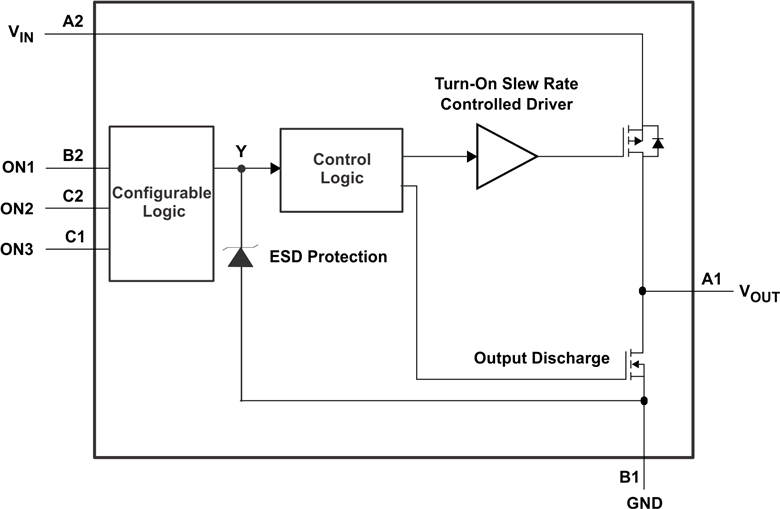
The TPS22932B device is a low rONload switch with controlled turnon. The device contains a P-channel MOSFET that can operate over an input voltage range of 1.1 V to 3.6 V.
The switch is controlled by eight patterns of 3-bit input. The user can choose the logic functions MUX, AND, OR, NAND, NOR, inverter, and noninverter. All inputs can be connected to VINor GND. The control pins can be connected to low-voltage GPIOs allowing the switch to be controlled by either 1.2-V, 1.8-V, 2.5-V, or 3.3-V logic signals while keeping extremely low quiescent current.
A 120-Ω on-chip load resistor is available for output quick discharge when the switch is turned off. The rise time (slew rate) of the device is internally controlled to avoid inrush current: the rise time of TPS22932B is 165 µs.
TPS22932B is available in a space-saving 6-pin DSBGA (YFP with 0.4-mm pitch). The device is characterized for operation over the free-air temperature range of –40°C to 85°C.


