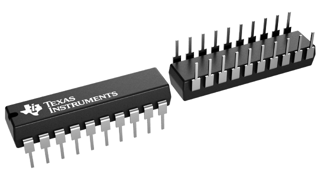
SN74HCT377 Series
High Speed CMOS Logic Octal D-Type Flip-Flop with Data Enable
Manufacturer: Texas Instruments
Catalog
High Speed CMOS Logic Octal D-Type Flip-Flop with Data Enable
Key Features
• Buffered Common ClockBuffered InputsTypical Propagation Delay at CL= 15pF, VCC= 5V, TA= 25°C14 ns (HC Types)16 ns (HCT Types)Fanout (Over Temperature Range)Standard Outputs. . . . . . . . . . . . . . . 10 LSTTL LoadsBus Driver Outputs . . . . . . . . . . . . . 15 LSTTL LoadsWide Operating Temperature Range . . . –55°C to 125°CBalanced Propagation Delay and Transition TimesSignificant Power Reduction Compared to LSTTL Logic ICsHC Types2V to 6V OperationHigh Noise Immunity: NIL= 30%, NIH= 30%of VCCat VCC= 5VHCT Types4.5V to 5.5V OperationDirect LSTTL Input Logic Compatibility, VIL= 0.8V (Max), VIH= 2V (Min)CMOS Input Compatibility, Il1µA at VOL, VOHBuffered Common ClockBuffered InputsTypical Propagation Delay at CL= 15pF, VCC= 5V, TA= 25°C14 ns (HC Types)16 ns (HCT Types)Fanout (Over Temperature Range)Standard Outputs. . . . . . . . . . . . . . . 10 LSTTL LoadsBus Driver Outputs . . . . . . . . . . . . . 15 LSTTL LoadsWide Operating Temperature Range . . . –55°C to 125°CBalanced Propagation Delay and Transition TimesSignificant Power Reduction Compared to LSTTL Logic ICsHC Types2V to 6V OperationHigh Noise Immunity: NIL= 30%, NIH= 30%of VCCat VCC= 5VHCT Types4.5V to 5.5V OperationDirect LSTTL Input Logic Compatibility, VIL= 0.8V (Max), VIH= 2V (Min)CMOS Input Compatibility, Il1µA at VOL, VOH
Description
AI
These devices are positive-edge-triggered D-type flip-flops. The ’HCT377 devices are similar to the ’'HCT273 devices, but feature a latched clock-enable (CLKEN)\ input instead of a common clear.
Information at the data (D) inputs meeting the setup time requirements is transferred to the Q outputs on the positive-going edge of the clock (CLK) pulse if CLKEN\ is low. Clock triggering occurs at a particular voltage level and is not directly related to the transition time of the positive-going pulse. When CLK is at either the high or low level, the D input has no effect at the output. These devices are designed to prevent false clocking by transitions at CLKEN\.


