Catalog
5 kV rms, 600 Mbps Dual Tx and Rx Channel LVDS Isolator
Key Features
• 5 kV rms/3.75 kV rms LVDS isolator
• Complies with TIA/EIA-644-A LVDS standard
• Multiple dual-channel configurations
• Up to 600 Mbps switching with low jitter4.5 ns maximum propagation delay151 ps maximum peak-to-peak total jitter at 600 Mbps100 ps maximum pulse skew600 ps maximum part to part skew
• 4.5 ns maximum propagation delay
• 151 ps maximum peak-to-peak total jitter at 600 Mbps
• 100 ps maximum pulse skew
• 600 ps maximum part to part skew
• 2.5 V or 3.3 V supplies
• −75 dBc power supply ripple rejection and glitch immunity
• ±8 kV IEC 61000-4-2 ESD protection across isolation barrier
• High common-mode transient immunity: >25 kV/μs
• Passes EN55022 Class B radiated emissions limits with 600 Mbps PRBS
• Safety and regulatory approvals (20-lead SOIC package)UL: 5000 V rms for 1 minute per UL 1577CSA Component Acceptance Notice 5AVDE certificate of conformityDIN V VDE V 0884-10 (VDE V 0884-10):2006-12VIORM = 424 V peak
• UL: 5000 V rms for 1 minute per UL 1577
• CSA Component Acceptance Notice 5A
• VDE certificate of conformityDIN V VDE V 0884-10 (VDE V 0884-10):2006-12VIORM = 424 V peak
• DIN V VDE V 0884-10 (VDE V 0884-10):2006-12
• VIORM = 424 V peak
• Fail-safe output high for open, short, and terminated input conditions
• Operating temperature range: −40°C to +125°C
• Choice of package and isolation options3.75 kV rms in highly integrated 20-lead SSOP5 kV rms in 20-lead SOIC with 7.8 mm creepage/clearance
• 3.75 kV rms in highly integrated 20-lead SSOP
• 5 kV rms in 20-lead SOIC with 7.8 mm creepage/clearance
Description
AI
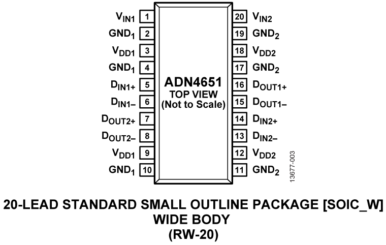
TheADN4650/ADN4651/ADN46521are signal isolated, low voltage differential signaling (LVDS) buffers that operate at up to 600 Mbps with very low jitter.The devices integrate Analog Devices, Inc.,iCoupler®technology, enhanced for high speed operation, to provide galvanic isolation of the TIA/EIA-644-A compliant LVDS drivers and receivers. This technology allows drop-in isolation of an LVDS signal chain.Multiple channel configurations are offered, and the LVDS receivers on the ADN4651/ADN4652 include a fail-safe mechanism to ensure a Logic 1 on the corresponding LVDS driver output when the inputs are floating, shorted, or terminated, but not driven.For high speed operation with low jitter, the LVDS and isolator circuits rely on a 2.5 V supply. An integrated on-chip low dropout regulator (LDO) can provide the required 2.5 V from an external 3.3 V power supply. The devices are fully specified over a wide industrial temperature range and are available in a 20-lead, wide body SOIC package with 5 kV rms isolation or a 20-lead SSOP package with 3.75 kV rms isolation.ApplicationsAnalog front-end (AFE) isolationData plane isolationIsolated high speed clock and data linksIsolated serial peripheral interface (SPI) over LVDS


