ADN4622 Series
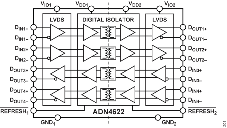
5.7 kV rms/1.5 kV rms, Quad-Channel LVDS 2.5 Gigabit Isolators (2 Reverse Channels)
Manufacturer: Analog Devices
Catalog
5.7 kV rms/1.5 kV rms, Quad-Channel LVDS 2.5 Gigabit Isolators (2 Reverse Channels)
Key Features
• 5.7 kV rms and 1.5 kV rms LVDS isolators
• Complies with TIA/EIA-644-A LVDS signal levels
• Quad-channel configuration (ADN4622: 2 + 2, ADN4624: 4 + 0)
• Any data rate up to 2.5 Gbps switching with low jitter10 Gbps total bandwidth across four channels2.15 ns typical propagation delayTypical jitter: 0.82 ps rms random, 40 ps total peak
• 10 Gbps total bandwidth across four channels
• 2.15 ns typical propagation delay
• Typical jitter: 0.82 ps rms random, 40 ps total peak
• Lower power 1.8 V supplies
• ±8 kV IEC 61000-4-2 ESD protection across isolation barrier
• High common-mode transient immunity: 100 kV/μs typical
• Safety and regulatory approvals (28-lead SOIC_W_FP package)UL (pending): 5700 V rms for 1 minute per UL 1577CSA Component Acceptance Notice 5A (pending)VDE certificate of conformity (pending)DIN V VDE V 0884-11 (VDE V 0884-11):2017-01VIORM= 849 VPEAK(working voltage)
• UL (pending): 5700 V rms for 1 minute per UL 1577
• CSA Component Acceptance Notice 5A (pending)
• VDE certificate of conformity (pending)DIN V VDE V 0884-11 (VDE V 0884-11):2017-01VIORM= 849 VPEAK(working voltage)
• DIN V VDE V 0884-11 (VDE V 0884-11):2017-01
• VIORM= 849 VPEAK(working voltage)
• Enable or disable refresh (low-speed output correctness check)
• Operating temperature range: −40°C to +125°C
• 28-lead, wide-body, finer pitch SOIC_W_FP package with 8.3 mm creepage and clearance or 6 mm × 6 mm LFCSP package with 1.27 mm creepage and clearance
Description
AI
The ADN4622/ADN4624are quad-channel, signal isolated, low-voltage differential signaling (LVDS) buffers that operate at up to 2.5 Gbps with very low jitter. The devices integrate Analog Devices, Inc.,iCoupler®technology, enhanced for high-speed operation to provide drop-in galvanic isolation of LVDS signal chains. AC coupling and/or level shifting to the LVDS receivers and from the LVDS drivers allows isolation of other high-speed signals such as current-mode logic (CML).The ADN4622/ADN4624 include a refresh mechanism to monitor the input and output states and ensure they remain the same in the absence of data transitions. For lower power consumption and high-speed operation with low jitter, the LVDS and isolator circuits rely on 1.8 V supplies. The ADN4622/ADN4624 are fully specified over a wide industrial temperature range and are available in a 28-lead, wide-body, finer pitch SOIC_W_FP package with 8.3 mm creepage and clearance (for 5.7 kV rms or 8 kVPEAKsurge and impulse voltages and reinforced insulation at AC mains voltages) or 6 mm × 6 mm LFCSP package with 1.27 mm creepage and clearance (for basic/functional isolation).APPLICATIONSIsolated video and imaging dataAnalog front-end isolationData plane isolationIsolated high speed clock and data linksMulti-gigabit SERDESBoard-to-board optical replacement (for example, short reach fiber)


