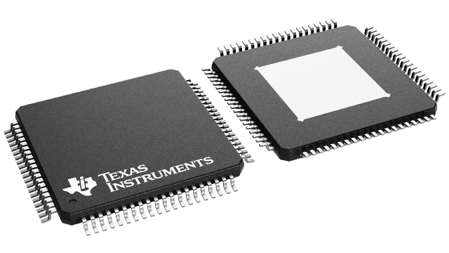
ADS5444-SP Series
13-bit 250-MSPS analog-to-digital converter (ADC) - enhanced product
Manufacturer: Texas Instruments
Catalog
13-bit 250-MSPS analog-to-digital converter (ADC) - enhanced product
Key Features
• Controlled BaselineOne AssemblyOne Test SiteOne Fabrication SiteExtended Temperature Performance of -55°C to 125°CEnhanced Diminishing Manufacturing Sources (DMS) SupportEnhanced Product-Change NotificationQualification Pedigree(1)13-Bit Resolution250-MSPS Sample RateSNR = 69 dBc at 100-MHz IF and 250 MSPSSFDR = 76 dBc at 100-MHz IF and 250 MSPSSNR = 67.7 dBc at 230-MHz IF and 250 MSPSSFDR = 77 dBc at 230-MHz IF and 250 MSPS2.2-VPPDifferential Input VoltageFully Buffered Analog Inputs5-V Analog Supply VoltageLVDS Compatible OutputsTotal Power Dissipation: 2 WOffset Binary Output FormatTQFP-80 PowerPAD™ PackagePin Compatible With the ADS5440Military Temperature Range = -55°C to 125°CAPPLICATIONSTest and MeasurementSoftware-Defined RadioMultichannel Base Station ReceiversBase Station Tx Digital PredistortionCommunications InstrumentationRELATED PRODUCTSADS5424 - 14-Bit, 105 MSPS ADCADS5423 - 14-Bit, 80 MSPS ADCADS5440 - 13-Bit, 210 MSPS ADC(1)Component qualification in accordance with JEDEC and industry standards to ensure reliable operation over an extended temperature range. This includes, but is not limited to, Highly Accelerated Stress Test (HAST) or biased 85/85, temperature cycle, autoclave or unbiased HAST, electromigration, bond intermetallic life, and mold compound life. Such qualification testing should not be viewed as justifying use of this component beyond specified performance and environmental limits.PowerPAD is a trademark of Texas Instruments.Controlled BaselineOne AssemblyOne Test SiteOne Fabrication SiteExtended Temperature Performance of -55°C to 125°CEnhanced Diminishing Manufacturing Sources (DMS) SupportEnhanced Product-Change NotificationQualification Pedigree(1)13-Bit Resolution250-MSPS Sample RateSNR = 69 dBc at 100-MHz IF and 250 MSPSSFDR = 76 dBc at 100-MHz IF and 250 MSPSSNR = 67.7 dBc at 230-MHz IF and 250 MSPSSFDR = 77 dBc at 230-MHz IF and 250 MSPS2.2-VPPDifferential Input VoltageFully Buffered Analog Inputs5-V Analog Supply VoltageLVDS Compatible OutputsTotal Power Dissipation: 2 WOffset Binary Output FormatTQFP-80 PowerPAD™ PackagePin Compatible With the ADS5440Military Temperature Range = -55°C to 125°CAPPLICATIONSTest and MeasurementSoftware-Defined RadioMultichannel Base Station ReceiversBase Station Tx Digital PredistortionCommunications InstrumentationRELATED PRODUCTSADS5424 - 14-Bit, 105 MSPS ADCADS5423 - 14-Bit, 80 MSPS ADCADS5440 - 13-Bit, 210 MSPS ADC(1)Component qualification in accordance with JEDEC and industry standards to ensure reliable operation over an extended temperature range. This includes, but is not limited to, Highly Accelerated Stress Test (HAST) or biased 85/85, temperature cycle, autoclave or unbiased HAST, electromigration, bond intermetallic life, and mold compound life. Such qualification testing should not be viewed as justifying use of this component beyond specified performance and environmental limits.PowerPAD is a trademark of Texas Instruments.
Description
AI
The ADS5444 is a 13 bit 250 MSPS analog-to-digital converter (ADC) that operates from a 5 V supply, while providing LVDS-compatible digital outputs from a 3.3 V supply. The ADS5444 input buffer isolates the internal switching of the onboard track and hold (T&H) from disturbing the signal source. An internal reference generator is also provided to further simplify the system design. The ADS5444 has outstanding low noise and linearity over input frequency.
The ADS5444 is available in a 84 pin ceramic nonconductive tie-bar package (HFG). The ADS5444 is built on a state-of-the-art Texas Instruments complementary bipolar process (BiCom3X) and is specified over the full military temperature range (–55°C to 125°C Tcase).
This CQFP package has built in vias that electrically and thermally connect the bottom of the die to a pad on the bottom of the package. To efficiently remove heat and provide a low-impedance ground path, a thermal land is required on the surface of the PCB directly underneath the body of the package. During normal surface mount flow solder operations, the heat pad on the underside of the package is soldered to this thermal land creating an efficient thermal path. Normally, the PCB thermal land has a number of thermal vias within it that provide a thermal path to internal copper areas (or to the opposite side of the PCB) that provide for more efficient heat removal. TI typically recommends an 11,9-mm2board-mount thermal pad. This allows maximum area for thermal dissipation, while keeping leads away from the pad area to prevent solder bridging. A sufficient quantity of thermal/electrical vias must be included to keep the device within recommended operating conditions. This pad must be electrically at ground potential.


