ADS5294 Series
Eight-Channel, 14-Bit, 80-MSPS Analog-to-Digital Converter (ADC)
Manufacturer: Texas Instruments
Catalog
Eight-Channel, 14-Bit, 80-MSPS Analog-to-Digital Converter (ADC)
Key Features
• Maximum Sample Rate: 80 MSPS/14-BitHigh Signal-to-Noise Ratio75.5-dBFS SNR at 5 MHz / 80 MSPS78.2-dBFS SNR at 5 MHz / 80 MSPS and Decimation Filter Enabled84-dBc SFDR at 5 MHz / 80 MSPSLow Power Consumption58 mW/CH at 50 MSPS77 mW/CH at 80 MSPS (2-LVDS Wire Per Channel)Digital Processing BlockProgrammable FIR Decimation Filter and Oversampling to Minimize Harmonic InterferenceProgrammable IIR High-Pass Filter to Minimize DC OffsetProgrammable Digital Gain: 0 dB to 12 dB2-Channel or 4-Channel AveragingFlexible Serialized LVDS Outputs:One or Two Wires of LVDS Output Lines Per Channel Depending on ADC Sampling RateProgrammable Mapping Between ADC Input Channels and LVDS Output Pins-Eases Board DesignVariety of Test Patterns to Verify Data Capture by FPGA/ReceiverInternal and External References1.8-V Operation for Low Power ConsumptionLow-Frequency Noise SuppressionRecovery From 6-dB Overload Within 1 Clock CyclePackage: 12-mm × 12-mm 80-Pin QFPMaximum Sample Rate: 80 MSPS/14-BitHigh Signal-to-Noise Ratio75.5-dBFS SNR at 5 MHz / 80 MSPS78.2-dBFS SNR at 5 MHz / 80 MSPS and Decimation Filter Enabled84-dBc SFDR at 5 MHz / 80 MSPSLow Power Consumption58 mW/CH at 50 MSPS77 mW/CH at 80 MSPS (2-LVDS Wire Per Channel)Digital Processing BlockProgrammable FIR Decimation Filter and Oversampling to Minimize Harmonic InterferenceProgrammable IIR High-Pass Filter to Minimize DC OffsetProgrammable Digital Gain: 0 dB to 12 dB2-Channel or 4-Channel AveragingFlexible Serialized LVDS Outputs:One or Two Wires of LVDS Output Lines Per Channel Depending on ADC Sampling RateProgrammable Mapping Between ADC Input Channels and LVDS Output Pins-Eases Board DesignVariety of Test Patterns to Verify Data Capture by FPGA/ReceiverInternal and External References1.8-V Operation for Low Power ConsumptionLow-Frequency Noise SuppressionRecovery From 6-dB Overload Within 1 Clock CyclePackage: 12-mm × 12-mm 80-Pin QFP
Description
AI
The ADS5294 is a low-power 80-MSPS 8-Channel ADC that uses CMOS process technology and innovative circuit techniques. Low power consumption, high SNR, low SFDR, and consistent overload recovery allow users to design high-performance systems.
The digital processing block of the ADS5294 integrates several commonly used digital functions for improving system performance. The device includes a digital filter module that has built-in decimation filters (with lowpass, highpass and bandpass characteristics). The decimation rate is also programmable (by 2, by 4, or by 8). This rate is useful for narrow-band applications, where the filters are used to conveniently improve SNR and knock-off harmonics, while at the same time reducing the output data rate. The device includes an averaging mode where two channels (or even four channels) are averaged to improve SNR.
Serial LVDS outputs reduce the number of interface lines and enable the highest system integration. The digital data from each channel ADC is output over one or two wires of LVDS output lines depending on the ADC sampling rate. This 2-wire interface maintains a low serial-data rate, allowing low-cost FPGA-based receivers to be used even at a high sample rate. The ADC resolution is programmed to 12-bit or 14-bit through registers. A unique feature is the programmable-mapping module that allows flexible mapping between the input channels and the LVDS output pins. This module greatly reduces the complexity of LVDS-output routing, and by reducing the number of PCB layers, potentially results in cheaper system boards.
The device integrates an internal reference trimmed to accurately match across devices. Internal reference mode achieves the best performance. External references can also drive the device.
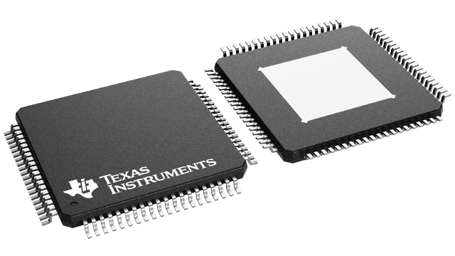
The device is available in a 12-mm × 12-mm 80-pin QFP package. The device is specified over a –40°C to 85°C operating temperature range. ADS5294 is completely pin-to-pin and register compatible to ADS5292.


