LMG1205 Series
1.2-A, 5-A 90-V, half bridge gate driver with 5-V UVLO for GaNFET and MOSFET
Manufacturer: Texas Instruments
Catalog
1.2-A, 5-A 90-V, half bridge gate driver with 5-V UVLO for GaNFET and MOSFET
Key Features
• Independent high-side and low-side TTL logic inputs1.2-A peak source, 5-A sink currentHigh-side floating bias voltage rail operates up to 100 VDCInternal bootstrap supply voltage clampingSplit outputs for adjustable turnon, turnoff strength0.6-Ω pulldown, 2.1-Ω pullup resistanceFast propagation times (35 ns typical)Excellent propagation delay matching (1.5 ns typical)Supply rail undervoltage lockoutLow power consumptionIndependent high-side and low-side TTL logic inputs1.2-A peak source, 5-A sink currentHigh-side floating bias voltage rail operates up to 100 VDCInternal bootstrap supply voltage clampingSplit outputs for adjustable turnon, turnoff strength0.6-Ω pulldown, 2.1-Ω pullup resistanceFast propagation times (35 ns typical)Excellent propagation delay matching (1.5 ns typical)Supply rail undervoltage lockoutLow power consumption
Description
AI
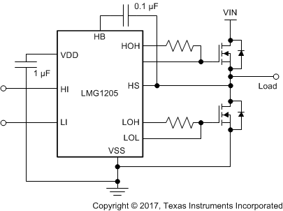
The LMG1205 is designed to drive both the high-side and the low-side enhancement mode Gallium Nitride (GaN) FETs in a synchronous buck, boost, or half-bridge configuration. The device has an integrated 100-V bootstrap diode and independent inputs for the high-side and low-side outputs for maximum control flexibility. The high-side bias voltage is generated using a bootstrap technique and is internally clamped at 5 V, which prevents the gate voltage from exceeding the maximum gate-source voltage rating of enhancement mode GaN FETs. The inputs of the LMG1205 are TTL logic compatible and can withstand input voltages up to 14 V regardless of the VDD voltage. The LMG1205 has split-gate outputs, providing flexibility to adjust the turnon and turnoff strength independently.
In addition, the strong sink capability of the LMG1205 maintains the gate in the low state, preventing unintended turnon during switching. The LMG1205 can operate up to several MHz. The LMG1205 is available in a 12-pin DSBGA package that offers a compact footprint and minimized package inductance.


