ISO6731-Q1 Series
Automotive, general-purpose, triple-channel, 2/1, digital isolator
Manufacturer: Texas Instruments
Catalog
Automotive, general-purpose, triple-channel, 2/1, digital isolator
Key Features
• Functional Safety-CapableDocumentation available to aid functional safety system design:ISO6731-Q1AEC-Q100 qualified with the following results:Device temperature Grade 1: –40°C to +125°C ambient operating temperature rangeMeets VDA320 isolation requirements50 Mbps data rateRobust isolation barrier:High lifetime at 1500 VRMSworking voltageUp to 5000 VRMSisolation ratingUp to 10 kV surge capability±75 kV/µs typical CMTIWide supply range: 1.71 V to 1.89 V and 2.25 V to 5.5 V1.71 V to 5.5 V level translationDefault outputhigh(ISO6731-Q1) andlow(ISO6731F-Q1) options1.6 mA per channel typical at 1 MbpsLow propagation delay: 11 ns typicalRobust electromagnetic compatibility (EMC)System-level ESD, EFT, and surge immunity±8 kV IEC 61000-4-2 contact discharge protection across isolation barrierLow emissionsWide-SOIC (DW-16) PackageSafety-Related Certifications:DIN VDE V 0884-11:2017-01UL 1577 component recognition programIEC 62368-1, IEC 61010-1, IEC 60601-1GB 4943.1-2011 certifications (pending)Functional Safety-CapableDocumentation available to aid functional safety system design:ISO6731-Q1AEC-Q100 qualified with the following results:Device temperature Grade 1: –40°C to +125°C ambient operating temperature rangeMeets VDA320 isolation requirements50 Mbps data rateRobust isolation barrier:High lifetime at 1500 VRMSworking voltageUp to 5000 VRMSisolation ratingUp to 10 kV surge capability±75 kV/µs typical CMTIWide supply range: 1.71 V to 1.89 V and 2.25 V to 5.5 V1.71 V to 5.5 V level translationDefault outputhigh(ISO6731-Q1) andlow(ISO6731F-Q1) options1.6 mA per channel typical at 1 MbpsLow propagation delay: 11 ns typicalRobust electromagnetic compatibility (EMC)System-level ESD, EFT, and surge immunity±8 kV IEC 61000-4-2 contact discharge protection across isolation barrierLow emissionsWide-SOIC (DW-16) PackageSafety-Related Certifications:DIN VDE V 0884-11:2017-01UL 1577 component recognition programIEC 62368-1, IEC 61010-1, IEC 60601-1GB 4943.1-2011 certifications (pending)
Description
AI
The ISO6731-Q1 device is a high-performance, triple-channel digital isolators ideal for cost-sensitive applications requiring up to 5000 VRMSisolation ratings per UL 1577. This device is also certified by VDE, TUV, CSA, and CQC.
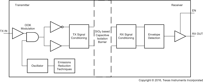
The ISO6731-Q1 devics provides high electromagnetic immunity and low emissions at low power consumption, while isolating CMOS or LVCMOS digital I/Os. Each isolation channel has a logic input and output buffer separated by TI’s double capacitive silicon dioxide (SiO2) insulation barrier. This device comes with enable pins which can be used to put the respective outputs in high impedance for multi-master driving applications. The ISO6731-Q1 device has two forward and one reverse-direction channels. In the event of input power or signal loss, the default output ishighfor the device without suffix F andlowfor the device with suffix F. See Device Functional Modes section for further details.
Used in conjunction with isolated power supplies, this device helps prevent noise currents on data buses, such as CAN and LIN from damaging sensitive circuitry. Through innovative chip design and layout techniques, the electromagnetic compatibility of the ISO6731-Q1 device has been significantly enhanced to ease system-level ESD, EFT, surge, and emissions compliance. The ISO6731-Q1 device is available in a 16-pin SOIC wide-body (DW) package and is a pin-to-pin upgrade to the older generations.


