ADN4654 Series
5 kV RMS/3.75 kV RMS, Dual LVDS Gigabit Isolator (0 Reverse Channels)
Manufacturer: Analog Devices
Catalog
5 kV RMS/3.75 kV RMS, Dual LVDS Gigabit Isolator (0 Reverse Channels)
Key Features
• 5 kV rms and 3.75 kV rms LVDS isolators
• Complies with TIA/EIA-644-A LVDS standard
• Multiple dual-channel configurations
• Any data rate up to 1.1 Gbps switching with low jitter4 ns typical propagation delay2.6 ps rms typical random jitter, rms90 ps typical peak-to-peak total jitter at 1.1 Gbps
• 4 ns typical propagation delay
• 2.6 ps rms typical random jitter, rms
• 90 ps typical peak-to-peak total jitter at 1.1 Gbps
• 2.5 V or 3.3 V supplies
• −75 dBc power supply ripple rejection, phase spur level
• Glitch immunity
• ±8 kV IEC 61000-4-2 ESD protection across isolation barrier
• High common-mode transient immunity: >25 kV/μs
• Passes EN 55022 Class B radiated emissions limits with 1.1 Gbps PRBS
• Safety and regulatory approvals (20-lead SOIC_W package)UL (pending): 5000 V rms for 1 minute per UL 1577CSA Component Acceptance Notice 5A (pending)VDE certificate of conformity (pending)DIN V VDE V 0884-10 (VDE V 0884-10):2006-12VIORM= 424 VPEAK
• UL (pending): 5000 V rms for 1 minute per UL 1577
• CSA Component Acceptance Notice 5A (pending)
• VDE certificate of conformity (pending)DIN V VDE V 0884-10 (VDE V 0884-10):2006-12VIORM= 424 VPEAK
• DIN V VDE V 0884-10 (VDE V 0884-10):2006-12
• VIORM= 424 VPEAK
• Fail-safe output high for open, short, and terminated input conditions (ADN4655/ADN4656)
• Operating temperature range: −40°C to +125°C
• 7.8 mm minimum creepage and clearance
Description
AI
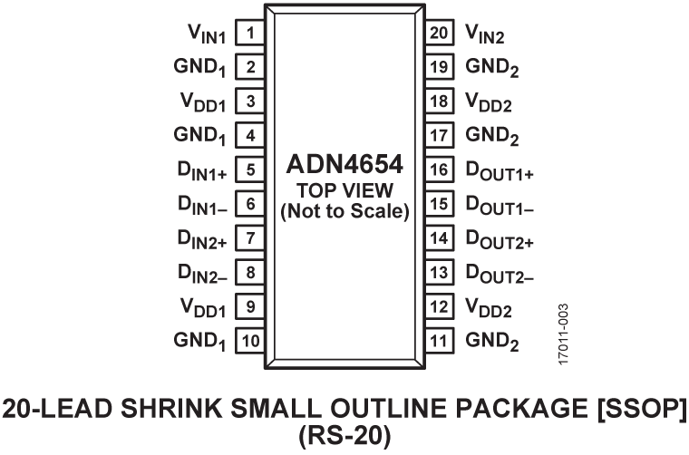
The ADN4654/ADN4655/ADN46561are signal isolated, low voltage differential signaling (LVDS) buffers that operate at up to 1.1 Gbps with low jitter. The devices integrate Analog Devices, Inc.,iCoupler®technology, enhanced for high speed operation to provide galvanic isolation of the TIA/EIA-644-A compliant LVDS drivers and receivers. This integration allows drop-in isolation of an LVDS signal chain.The ADN4654/ADN4655/ADN4656 comprise multiple channel configurations, and the LVDS receivers on the ADN4655 and ADN4656 include a fail-safe mechanism to ensure a Logic 1 on the corresponding LVDS driver output when the inputs are floating, shorted, or terminated but not driven.For high speed operation with low jitter, the LVDS and isolator circuits rely on a 2.5 V supply. An integrated on-chip low dropout (LDO) regulator can provide the required 2.5 V from an external 3.3 V power supply. The devices are fully specified over a wide industrial temperature range and come in a 20-lead, wide body SOIC_W package with 5 kV rms isolation or in a 20-lead SSOP package with 3.75 kV rms isolation.ApplicationsIsolated video and imaging dataAnalog front-end isolationData plane isolationIsolated high speed clock and data links1Protected by U.S. Patents 5,952,849; 6,873,065; 6,903,578; and 7,075,329. Other patents are pending.


