AD9652 Series
16-bit, 310 MSPS, 3.3/1.8 V Dual Analog-to-Digital Converter (ADC)
Manufacturer: Analog Devices
Catalog
16-bit, 310 MSPS, 3.3/1.8 V Dual Analog-to-Digital Converter (ADC)
Key Features
• High Dynamic RangeSNR = 75.0 dBFS at 70 MHz(AIN = −1 dBFS)SFDR = 87 dBc at 70 MHz(AIN = −1 dBFS)
• Excellent IF Sampling PerformanceSNR = 73.7 dBFS at 170 MHz (AIN= −1 dBFS)SFDR = 85 dBc at 170 MHz (AIN= −1 dBFS)Full power bandwidth of 465 MHz
• Energy saving power-down modes
• SYNC input allows multichip synchronization
• Differential clock input receiver with 1, 2, 4, and 8 integer inputs (clock divider input accepts up to 1.24 GHz)
• Internal ADC clock duty cycle stabilizer
• Total power consumption:2.16 W 3.3 V and 1.8 V supply voltages
• DDR LVDS (ANSI-644 levels) outputs
• Serial port control
• On-chip 3.3 V bufferProgrammable input span of 2 VP-Pto 2.5 VP-P(default)
Description
AI
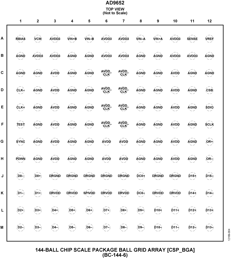
The AD9652 is a dual, 16-bit analog-to-digital converter (ADC) with sampling speeds of up to 310 MSPS. It is designed to support demanding, high speed signal processing applications that require exceptional dynamic range over a wide input frequency range (up to 465 MHz). Its exceptional low noise floor of −157.6 dBFS and large signal spurious-free dynamic range (SFDR) performance (exceeding 85 dBFS, typical) allows low level signals to be resolved in the presence of large signals.The dual ADC cores feature a multistage, pipelined architecture with integrated output error correction logic. A high performance on-chip buffer and internal voltage reference simplify the inter-face to external driving circuitry while preserving the exceptional performance of the ADC.The AD9652 can support input clock frequencies of up to 1.24 GHz with a 1, 2, 4, and 8 integer clock divider used to generate the ADC sample clock. A duty cycle stabilizer is provided to compensate for variations in the ADC clock duty cycle. The 16-bit output data (with an overrange bit) from each ADC is interleaved onto a single LVDS output port along with a double data rate (DDR) clock. Programming for setup and control are accomplished using a 3-wire SPI-compatible serial interface.The AD9652 is available in a 144-ball CSP_BGA and is specified over the industrial temperature range of −40°C to +85°C. This product is protected by pending U.S. patents.PRODUCT HIGHLIGHTSIntegrated dual, 16-bit, 310 MSPS ADCs.On-chip buffer simplifies ADC driver interface.Operation from a 3.3 V and 1.8 V supply and a separate digital output driver supply accommodating LVDS outputs.Proprietary differential input maintains excellent SNR performance for input frequencies of up to 485 MHz.SYNC input allows synchronization of multiple devices.Three-wire, 3.3 V or 1.8 V SPI port for register programming and readback.APPLICATIONSMiltary radar and communicationsMultimode digital receivers (3G or 4G)Test and InstrumentationSmart antenna systems


