Catalog
Automotive Catalog LVDS SERDES Transmitter
Key Features
• Controlled BaselineOne Assembly/Test Site, One Fabrication SiteEnhanced Diminishing ManufacturingSources (DMS) SupportEnhanced Product-Change NotificationQualification Pedigree21:3 Data Channel Compression at up to1.36 Gigabits per Second ThroughputSuited for Point-to-Point SubsystemCommunication With Very Low EMI21 Data Channels Plus Clock inLow-Voltage TTL and 3 Data Channels PlusClock Out Low-Voltage DifferentialOperates From a Single 3.3-V Supply and250 mW (Typ)5-V Tolerant Data Inputs’LVDS95 Has Rising Clock Edge Triggered InputsBus Pins Tolerate 6-kV HBM ESDPackaged in Thin Shrink Small-OutlinePackage With 20 Mil Terminal PitchConsumes <1 mW When DisabledWide Phase-Lock Input Frequency Range20 MHz to 68 MHzNo External Components Required for PLLInputs Meet or Exceed the Requirements ofANSI EIA/TIA-644 StandardIndustrial Temperature QualifiedTA= –40°C to 85°CReplacement for the National DS90CR215Component qualification in accordance with JEDEC and industry standards to ensure reliable operation over an extended temperature range. This includes, but is not limited to, Highly Accelerated Stress Test (HAST) or biased 85/85, temperature cycle, autoclave or unbiased HAST, electromigration, bond intermetallic life, and mold compound life. Such qualification testing should not be viewed as justifying use of this component beyond specified performance and environmental limits.Controlled BaselineOne Assembly/Test Site, One Fabrication SiteEnhanced Diminishing ManufacturingSources (DMS) SupportEnhanced Product-Change NotificationQualification Pedigree21:3 Data Channel Compression at up to1.36 Gigabits per Second ThroughputSuited for Point-to-Point SubsystemCommunication With Very Low EMI21 Data Channels Plus Clock inLow-Voltage TTL and 3 Data Channels PlusClock Out Low-Voltage DifferentialOperates From a Single 3.3-V Supply and250 mW (Typ)5-V Tolerant Data Inputs’LVDS95 Has Rising Clock Edge Triggered InputsBus Pins Tolerate 6-kV HBM ESDPackaged in Thin Shrink Small-OutlinePackage With 20 Mil Terminal PitchConsumes <1 mW When DisabledWide Phase-Lock Input Frequency Range20 MHz to 68 MHzNo External Components Required for PLLInputs Meet or Exceed the Requirements ofANSI EIA/TIA-644 StandardIndustrial Temperature QualifiedTA= –40°C to 85°CReplacement for the National DS90CR215Component qualification in accordance with JEDEC and industry standards to ensure reliable operation over an extended temperature range. This includes, but is not limited to, Highly Accelerated Stress Test (HAST) or biased 85/85, temperature cycle, autoclave or unbiased HAST, electromigration, bond intermetallic life, and mold compound life. Such qualification testing should not be viewed as justifying use of this component beyond specified performance and environmental limits.
Description
AI
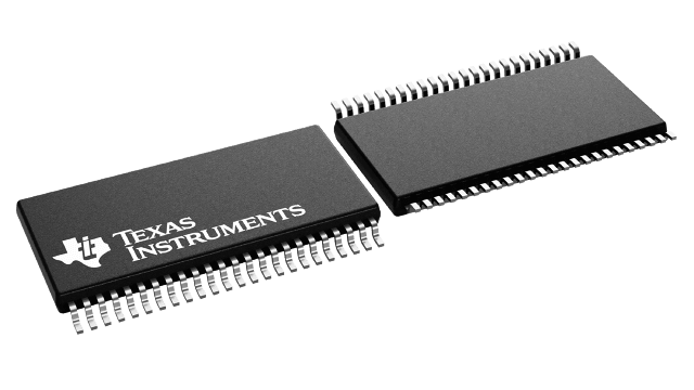
The SN65LVDS95 LVDS serdes (serializer/deserializer) transmitter contains three 7-bit parallel-load serial-out shift registers, a 7× clock synthesizer, and four low-voltage differential signaling (LVDS) line drivers in a single integrated circuit. These functions allow 21 bits of single-ended LVTTL data to be synchronously transmitted over 4 balanced-pair conductors for receipt by a compatible receiver, such as the SN65LVDS96.
When transmitting, data bits D0 through D20 are each loaded into registers of the SN65LVDS95 on the rising edge of the input clock signal (CLKIN). The frequency of CLKIN is multiplied seven times and then used to serially unload the data registers in 7-bit slices. The three serial streams and a phase-locked clock (CLKOUT) are then output to LVDS output drivers. The frequency of CLKOUT is the same as the input clock, CLKIN.
The SN65LVDS95 requires no external components and little or no control. The data bus appears the same at the input to the transmitter and output of the receiver with data transmission transparent to the user(s). The only user intervention is the possible use of the shutdown/clear (SHTDN) active-low input to inhibit the clock and shut off the LVDS output drivers for lower power consumption. A low level on this signal clears all internal registers to a low level.
The SN65LVDS95 is characterized for operation over ambient air temperatures of –40°C to 85°C.


