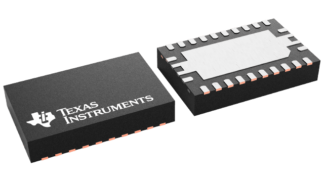
SN74AVC8T245-Q1 Series
Automotive Catalog 8-Bit Dual-Supply Bus Transceiver w/ Configurable Voltage Transl., 3-State Output
Manufacturer: Texas Instruments
Catalog
Automotive Catalog 8-Bit Dual-Supply Bus Transceiver w/ Configurable Voltage Transl., 3-State Output
Key Features
• Qualified for automotive applicationsAEC Q100 test guidance with the following results:Device temperature grade 1: –40°C to +125°C ambient operating temperature rangeDevice HBM ESD Classification Level H2Device CDM ESD Classification Level C3BControl inputs V IH and V IL levels are referenced to V CCA voltageV CC isolation feature – if either V CC input is at GND, all I/O ports are in the high-impedance stateI off supports partial power-down-mode operationFully configurable dual-rail design allows each port to operate over the full 1.4-V to 3.6-V power-supply rangeI/Os are 4.6-V tolerantMaximum data rates:170Mbps (V CCA < 1.8 V or V CCB < 1.8 V)320Mbps (V CCA ≥ 1.8 V and V CCB ≥ 1.8 V)Latch-up performance exceeds 100 mA per JESD 78, Class IIQualified for automotive applicationsAEC Q100 test guidance with the following results:Device temperature grade 1: –40°C to +125°C ambient operating temperature rangeDevice HBM ESD Classification Level H2Device CDM ESD Classification Level C3BControl inputs V IH and V IL levels are referenced to V CCA voltageV CC isolation feature – if either V CC input is at GND, all I/O ports are in the high-impedance stateI off supports partial power-down-mode operationFully configurable dual-rail design allows each port to operate over the full 1.4-V to 3.6-V power-supply rangeI/Os are 4.6-V tolerantMaximum data rates:170Mbps (V CCA < 1.8 V or V CCB < 1.8 V)320Mbps (V CCA ≥ 1.8 V and V CCB ≥ 1.8 V)Latch-up performance exceeds 100 mA per JESD 78, Class II
Description
AI
This 8-bit noninverting bus transceiver uses two separate configurable power-supply rails. The SN74AVC8T245 is optimized to operate with V CCA/V CCB set at 1.4 V to 3.6 V. The device is operational with V CCA and V CCB as low as 1.2 V. The A port is designed to track V CCA. V CCA accepts any supply voltage from 1.2 V to 3.6 V. The B port is designed to track V CCB. V CCB accepts any supply voltage from 1.2 V to 3.6 V. This allows for universal low-voltage bidirectional translation between any of the 1.2-V, 1.5-V, 1.8-V, 2.5-V, and 3.3-V voltage nodes.
The SN74AVC8T245 is designed for asynchronous communication between data buses. The device transmits data from the A bus to the B bus or from the B bus to the A bus, depending on the logic level at the direction-control (DIR) input. The output-enable ( OE) input can be used to disable the outputs so the buses are effectively isolated.
The SN74AVC8T245 is designed so that the control pins (DIR and OE) are supplied by V CCA.
The SN74AVC8T245 is compatible with a single-supply system and can be replaced later with a ’245 function, with minimal printed circuit board redesign.
This device is fully specified for partial-power-down applications using I off. The I off circuitry disables the outputs, thus preventing damaging current backflow through the device when it is powered down.
The V CC isolation feature allows both ports to be in the high-impedance state when either V CC input is at GND.
To put the device into the high-impedance state during power up or power down, tie OE to V CC through a pullup resistor; the current-sinking capability of the driver determines the minimum value of the resistor.


