LMG1210 Series
1.5-A, 3-A, 200-V half bridge gate driver, 5-V UVLO and programmable dead-time for GaNFET and MOSFET
Manufacturer: Texas Instruments
Catalog
1.5-A, 3-A, 200-V half bridge gate driver, 5-V UVLO and programmable dead-time for GaNFET and MOSFET
Key Features
• Up to 50-MHz operation10-ns typical propagation delay3.4-ns high-side to low-side matchingMinimum pulse width of 4 nsTwo control input optionsSingle PWM input with adjustable dead timeIndependent input mode1.5-A peak source and 3-A peak sink currentsExternal bootstrap diode for flexibilityInternal LDO for adaptability to voltage railsHigh 300-V/ns CMTIHO to LO capacitance less than 1 pFUVLO and overtemperature protectionLow-inductance WQFN packageUp to 50-MHz operation10-ns typical propagation delay3.4-ns high-side to low-side matchingMinimum pulse width of 4 nsTwo control input optionsSingle PWM input with adjustable dead timeIndependent input mode1.5-A peak source and 3-A peak sink currentsExternal bootstrap diode for flexibilityInternal LDO for adaptability to voltage railsHigh 300-V/ns CMTIHO to LO capacitance less than 1 pFUVLO and overtemperature protectionLow-inductance WQFN package
Description
AI
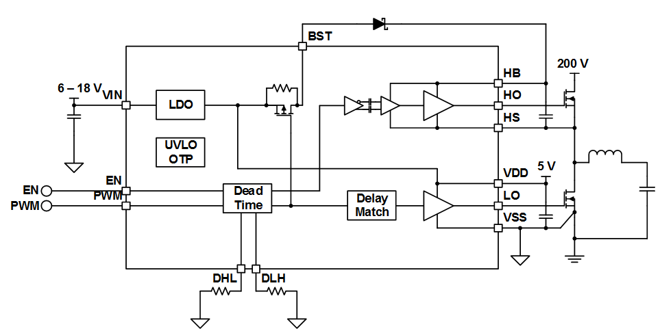
The LMG1210 is a 200-V, half-bridge MOSFET and Gallium Nitride Field Effect Transistor (GaN FET) driver designed for ultra-high frequency, high-efficiency applications that features adjustable deadtime capability, very small propagation delay, and 3.4-ns high-side low-side matching to optimize system efficiency. This part also features an internal LDO which ensures a gate-drive voltage of 5-V regardless of supply voltage.
To enable best performance in a variety of applications, the LMG1210 allows the designer to choose the optimal bootstrap diode to charge the high-side bootstrap capacitor. An internal switch turns the bootstrap diode off when the low side is off, effectively preventing the high-side bootstrap from overcharging and minimizing the reverse recovery charge. Additional parasitic capacitance across the GaN FET is minimized to less than 1 pF to reduce additional switching losses.
The LMG1210 features two control input modes: Independent Input Mode (IIM) and PWM mode. In IIM each of the outputs is independently controlled by a dedicated input. In PWM mode the two complementary output signals are generated from a single input and the user can adjust the dead time from 0 to 20 ns for each edge. The LMG1210 operates over a wide temperature range from –40°C to 125°C and is offered in a low-inductance WQFN package.


