DS90C383B Series
3.3-V programmable LVDS transmitter 24-bit flat panel display (FPD-Link) - 65 MHz
Manufacturer: Texas Instruments
Catalog
3.3-V programmable LVDS transmitter 24-bit flat panel display (FPD-Link) - 65 MHz
Key Features
• No special start-up sequence required between clock/data and /PD pins. Input signal (clock and data) can be applied either before or after the device is poweredSupport Spread Spectrum Clocking up to 100kHz frequency modulation and deviations of ±2.5% center spread or -5% down spread"Input Clock Detection" feature will pull all LVDS pairs to logic low when input clock is missing and when /PD pin is logic high18 to 68 MHz shift clock supportBest-in-Class Setup and Hold Times on TxINPUTsTx power consumption < 130 mW (typ) at 65MHz Grayscale40% Less Power Dissipation than BiCMOS AlternativesTx Power-down mode < 60μW (typ)Supports VGA, SVGA, XGA and Dual Pixel SXGA.Narrow bus reduces cable size and costUp to 1.8 Gbps throughputUp to 227 Megabytes/sec bandwidth345 mV (typ) swing LVDS devices for low EMIPLL requires no external componentsCompatible with TIA/EIA-644 LVDS standardLow profile 56-lead TSSOP packageImproved replacement for:SN75LVDS83, DS90C383AAll trademarks are the property of their respective owners. TRI-STATE is a trademark of Texas Instruments. TRI-STATE is a trademark of Texas Instruments.No special start-up sequence required between clock/data and /PD pins. Input signal (clock and data) can be applied either before or after the device is poweredSupport Spread Spectrum Clocking up to 100kHz frequency modulation and deviations of ±2.5% center spread or -5% down spread"Input Clock Detection" feature will pull all LVDS pairs to logic low when input clock is missing and when /PD pin is logic high18 to 68 MHz shift clock supportBest-in-Class Setup and Hold Times on TxINPUTsTx power consumption < 130 mW (typ) at 65MHz Grayscale40% Less Power Dissipation than BiCMOS AlternativesTx Power-down mode < 60μW (typ)Supports VGA, SVGA, XGA and Dual Pixel SXGA.Narrow bus reduces cable size and costUp to 1.8 Gbps throughputUp to 227 Megabytes/sec bandwidth345 mV (typ) swing LVDS devices for low EMIPLL requires no external componentsCompatible with TIA/EIA-644 LVDS standardLow profile 56-lead TSSOP packageImproved replacement for:SN75LVDS83, DS90C383AAll trademarks are the property of their respective owners. TRI-STATE is a trademark of Texas Instruments. TRI-STATE is a trademark of Texas Instruments.
Description
AI
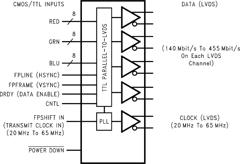
The DS90C383 transmitter converts 28 bits of CMOS/TTL data into four LVDS (Low Voltage Differential Signaling) data streams. A phase-locked transmit clock is transmitted in parallel with the data streams over a fifth LVDS link. Every cycle of the transmit clock 28 bits of input data are sampled and transmitted. The DS90CF384 receiver converts the LVDS data streams back into 28 bits of CMOS/TTL data. At a transmit clock frequency of 65 MHz, 24 bits of RGB data and 3 bits of LCD timing and control data (FPLINE, FPFRAME, DRDY) are transmitted at a rate of 455 Mbps per LVDS data channel. Using a 65 MHz clock, the data throughputs is 227 Mbytes/sec. The transmitter is offered with programmable edge data strobes for convenient interface with a variety of graphics controllers. The transmitter can be programmed for Rising edge strobe or Falling edge strobe through a dedicated pin. A Rising edge transmitter will inter-operate with a Falling edge receiver (DS90CF384) without any translation logic. The DS90CF384 is also offered in 64 ball, 0.8mm fine pitch ball grid array(FBGA) package which provides a 44 % reduction in PCB footprint (available Q3, 1999).
This chipset is an ideal means to solve EMI and cable size problems associated with wide, high speed TTL interfaces.


