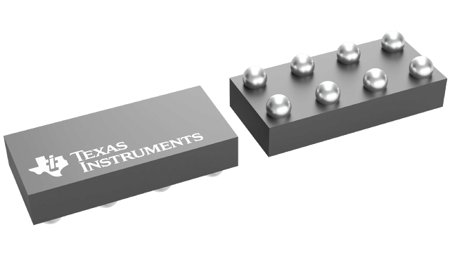
SN74LVC2G241 Series
2-ch, 1.65-V to 5.5-V buffers with 3-state outputs
Manufacturer: Texas Instruments
Catalog
2-ch, 1.65-V to 5.5-V buffers with 3-state outputs
Key Features
• Available in the Texas InstrumentsNanoFree™ PackageSupports 5-V VCCOperationInputs Accept Voltages to 5.5 VMax tpdof 4.1 ns at 3.3 VLow Power Consumption, 10-µA Maximum ICC±24-mA Output Drive at 3.3 VTypical VOLP(Output Ground Bounce)<0.8 V at VCC= 3.3 V, TA= 25°CTypical VOHV(Output VOHUndershoot)>2 V at VCC= 3.3 V, TA= 25°CIoffSupports Live Insertion, Partial-Power-Down Mode, and Back-Drive ProtectionCan Be Used as a Down Translator to Translate Inputs From a Max of 5.5 V Downto the VCCLevelLatch-Up Performance Exceeds 100 mA PerJESD 78, Class IIESD Protection Exceeds JESD 222000-V Human-Body Model (A114-A)200-V Machine Model (A115-A)1000-V Charged-Device Model (C101)Available in the Texas InstrumentsNanoFree™ PackageSupports 5-V VCCOperationInputs Accept Voltages to 5.5 VMax tpdof 4.1 ns at 3.3 VLow Power Consumption, 10-µA Maximum ICC±24-mA Output Drive at 3.3 VTypical VOLP(Output Ground Bounce)<0.8 V at VCC= 3.3 V, TA= 25°CTypical VOHV(Output VOHUndershoot)>2 V at VCC= 3.3 V, TA= 25°CIoffSupports Live Insertion, Partial-Power-Down Mode, and Back-Drive ProtectionCan Be Used as a Down Translator to Translate Inputs From a Max of 5.5 V Downto the VCCLevelLatch-Up Performance Exceeds 100 mA PerJESD 78, Class IIESD Protection Exceeds JESD 222000-V Human-Body Model (A114-A)200-V Machine Model (A115-A)1000-V Charged-Device Model (C101)
Description
AI
This dual buffer and line driver is designed for 1.65-V to 5.5-V VCCoperation.
The SN74LVC2G241 device is designed specifically to improve both the performance and density of 3-state memory-address drivers, clock drivers, and bus-oriented receivers and transmitters.
NanoFree package technology is a major breakthrough in IC packaging concepts, using the die as the package.
The SN74LVC2G241 device is organized as two 1-bit line drivers with separate output-enable (1OE, 2OE) inputs. When 1OEis low and 2OE is high, the device passes data from the A inputs to the Y outputs. When 1OEis high and 2OE is low, the outputs are in the high-impedance state.
To ensure the high-impedance state during power up or power down,OEshould be tied to VCCthrough a pullup resistor, and OE should be tied to GND through a pulldown resistor; the minimum value of the resistor is determined by the current-sinking or the current-sourcing capability of the driver.
This device is fully specified for partial-power-down applications using Ioff. The Ioffcircuitry disables the outputs, preventing damaging current backflow through the device when it is powered down.


