Catalog
Ultralow Noise Drivers for Low Voltage ADCs
Key Features
• Low input voltage noise: 1.2 nV/√Hz
• Low common-mode output: 0.9 V on single supply
• Extremely low harmonic distortion−104 dBc HD2 at 10 MHz−79 dBc HD2 at 70 MHz−73 dBc HD2 at 100 MHz−101 dBc HD3 at 10 MHz−82 dBc HD3 at 70 MHz−75 dBc HD3 at 100 MHz
• −104 dBc HD2 at 10 MHz
• −79 dBc HD2 at 70 MHz
• −73 dBc HD2 at 100 MHz
• −101 dBc HD3 at 10 MHz
• −82 dBc HD3 at 70 MHz
• −75 dBc HD3 at 100 MHz
• High speed−3 dB bandwidth of 1.35 GHz, G = 1Slew rate: 3400 V/μs, 25% to 75%0.1 dB gain flatness to 380 MHzFast overdrive recovery of 1.5 ns
• −3 dB bandwidth of 1.35 GHz, G = 1
• Slew rate: 3400 V/μs, 25% to 75%
• 0.1 dB gain flatness to 380 MHz
• Fast overdrive recovery of 1.5 ns
• 0.5 mV typical offset voltage
• Externally adjustable gain
• Differential-to-differential or single-ended-to-differential operation
• Adjustable output common-mode voltage
• Single-supply operation: 3.3 V or 5 V
Description
AI
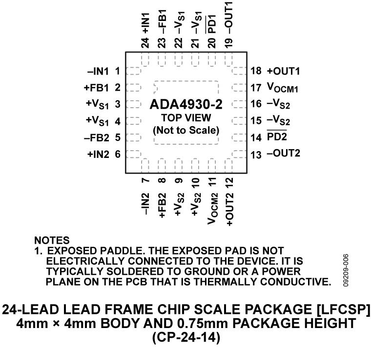
The ADA4930-1/ADA4930-2are very low noise, low distortion, high speed differential amplifiers. They are an ideal choice for driving 1.8 V high performance ADCs with resolutions up to 14 bits from dc to 70 MHz. The adjustable output common mode allows the ADA4930-1/ADA4930-2 to match the input of the ADC. The internal common-mode feedback loop provides exceptional output balance, suppression of even-order harmonic distortion products, and dc level translation.With the ADA4930-1/ADA4930-2, differential gain configurations are easily realized with a simple external feedback network of four resistors determining the closed-loop gain of the amplifier.The ADA4930-1/ADA4930-2 are fabricated using Analog Devices, Inc., proprietary silicon-germanium (SiGe), complementary bipolar process, enabling them to achieve very low levels of distortion with an input voltage noise of only 1.2 nV/√Hz.The low dc offset and excellent dynamic performance of the ADA4930-1/ADA4930-2 make them well suited for a wide variety of data acquisition and signal processing applications.The ADA4930-1 is available in a Pb-free, 3 mm × 3 mm 16-lead LFCSP, and the ADA4930-2 is available in a Pb-free, 4 mm × 4 mm 24-lead LFCSP. The pinout has been optimized to facilitate printed circuit board (PCB) layout and minimize distortion. The ADA4930-1 is specified to operate over the −40°C to +105°C temperature range, and the ADA4930-2 is specified to operate over the −40°C to +105°C temperature range for 3.3 V or 5 V supply voltages.ApplicationsADC driversSingle-ended-to-differential convertersIF and baseband gain blocksDifferential buffersLine drivers


