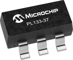
PL133-37 Series
Manufacturer: Microchip Technology
Catalog
Key Features
• + 3 LVCMOS Outputs
• + 12mA Output Drive Strength
• + Input/Output Frequency: Reference Clock: 1MHz to 150MHz
• + Supports LVCMOS or Sine Wave Input Clock
• + Very Low Jitter and Phase Noise
• + Low Current Consumption
• + Single 1.8V, 2.5V or 3.3V ±10% operation
• + 0°C to 70°C (Commercial)
• + -40°C to 85°C (Industrial)
• + Available in SOT23-6L GREEN/RoHS Compliant Packages
Description
AI
The PL133-37 is an advanced inverting fanout buffer design for high performance, low-power, small form-factor applications. The PL133-37 accepts a LVCMOS or a Sine Wave reference clock input of 1MHz to 150MHz and produces three outputs of the same frequency. Reference clock inputs may be LVCMOS or sine-wave signals (the inputs are internally AC-coupled so no external components required). Offered in a small 3 x 3mm SOT23, the PL133-37 offers the best phase noise and jitter performance and lowest power con-consumption of any comparable IC.


