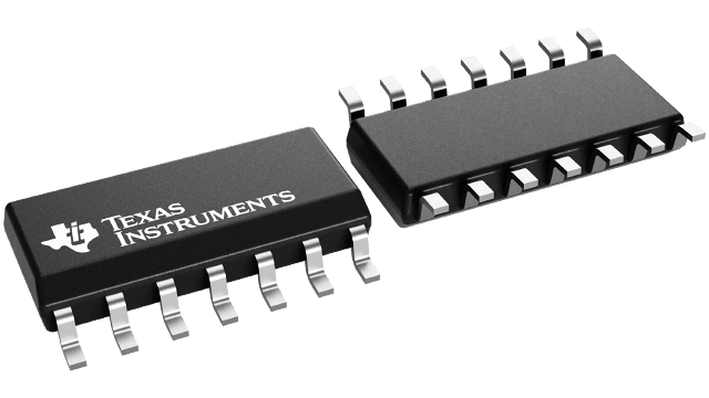
SN74CBT3125C Series
5-V, 1:1 (SPST), 4-channel general-purpose FET bus switch with st&ard '125-type pinout
Manufacturer: Texas Instruments
Catalog
5-V, 1:1 (SPST), 4-channel general-purpose FET bus switch with st&ard '125-type pinout
Key Features
• Undershoot Protection for Off-Isolation on A and B Ports Up To –2 VBidirectional Data Flow, With Near-Zero Propagation DelayLow On-State Resistance (ron) Characteristics(ron= 3Typical)Low Input/Output Capacitance Minimizes Loading and Signal Distortion(Cio(OFF)= 5 pF Typical)Data and Control Inputs Provide Undershoot Clamp DiodesLow Power Consumption(ICC= 3 µA Max)VCCOperating Range From 4 V to 5.5 VData I/Os Support 0 to 5-V Signaling Levels (0.8-V, 1.2-V, 1.5-V, 1.8-V, 2.5-V, 3.3-V, 5-V)Control Inputs Can Be Driven by TTL or 5-V/3.3-V CMOS OutputsIoffSupports Partial-Power-Down Mode OperationLatch-Up Performance Exceeds 100 mA Per JESD 78, Class IIESD Performance Tested Per JESD 222000-V Human-Body Model (A114-B, Class II)1000-V Charged-Device Model (C101)Supports Both Digital and Analog Applications: USB Interface, Bus Isolation, Low-Distortion Signal GatingUndershoot Protection for Off-Isolation on A and B Ports Up To –2 VBidirectional Data Flow, With Near-Zero Propagation DelayLow On-State Resistance (ron) Characteristics(ron= 3Typical)Low Input/Output Capacitance Minimizes Loading and Signal Distortion(Cio(OFF)= 5 pF Typical)Data and Control Inputs Provide Undershoot Clamp DiodesLow Power Consumption(ICC= 3 µA Max)VCCOperating Range From 4 V to 5.5 VData I/Os Support 0 to 5-V Signaling Levels (0.8-V, 1.2-V, 1.5-V, 1.8-V, 2.5-V, 3.3-V, 5-V)Control Inputs Can Be Driven by TTL or 5-V/3.3-V CMOS OutputsIoffSupports Partial-Power-Down Mode OperationLatch-Up Performance Exceeds 100 mA Per JESD 78, Class IIESD Performance Tested Per JESD 222000-V Human-Body Model (A114-B, Class II)1000-V Charged-Device Model (C101)Supports Both Digital and Analog Applications: USB Interface, Bus Isolation, Low-Distortion Signal Gating
Description
AI
The SN74CBT3125C is a high-speed TTL-compatible FET bus switch with low ON-state resistance (ron), allowing for minimal propagation delay. Active Undershoot-Protection Circuitry on the A and B ports of the SN74CBT3125C provides protection for undershoot up to –2 V by sensing an undershoot event and ensuring that the switch remains in the proper OFF state.
The SN74CBT3125C is organized as four 1-bit bus switches with separate output-enable (1OE\, 2OE\, 3OE\, 4OE\) inputs. It can be used as four 1-bit bus switches or as one 4-bit bus switch. When OE\ is low, the associated 1-bit bus switch is ON, and the A port is connected to the B port, allowing bidirectional data flow between ports. When OE\ is high, the associated 1-bit bus switch is OFF, and the high-impedance state exists between the A and B ports.
This device is fully specified for partial-power-down applications using Ioff. The Iofffeature ensures that damaging current will not backflow through the device when it is powered down.
To ensure the high-impedance state during power up or power down, OE\ should be tied to VCCthrough a pullup resistor; the minimum value of the resistor is determined by the current-sinking capability of the driver.


