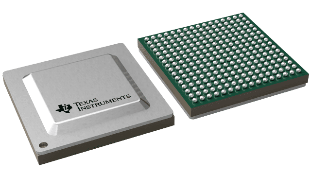
DAC12DL3200 Series
12-bit, low-latency, dual 3.2-GSPS or single 6.4-GSPS, RF-sampling DAC (LVDS interface)
Manufacturer: Texas Instruments
Catalog
12-bit, low-latency, dual 3.2-GSPS or single 6.4-GSPS, RF-sampling DAC (LVDS interface)
Key Features
• 12-bit resolutionMaximum input and output sample rate:Single channel up to 6.4 GSPSDual channel up to 3.2 GSPSMulti-Nyquist operating modes:Single channel modes: NRZ, RTZ, RFDual channel modes: NRZ, RTZ, RF, 2xRFLow latency through device: 6 to 8 nsMatching transmit capabilities to the low latency receiver ADC12DL3200DAC and ADC combined latency < 15 ns (not including FPGA)Parallel DDR LVDS interface:Source synchronous interface to simplify timing:24 or 48 LVDS pairs up to 1.6 Gbps1 LVDS DDR clock per 12-bit busOutput frequency range: > 8 GHzFull-scale current: 21 mASimplified clocking and synchronizationSYSREF windowing eases setup and hold timesOn-chip direct digital synthesizer (DDS)Single-tone and two-tone sine wave generation32 x 32-bit numerically controlled oscillatorsFast frequency hopping capability (< 500 ns)Synchronous CMOS frequency/phase inputPerformance at fOUT= 4.703 GHz, 6.4 GSPS, RF modeOutput power: –3 dBmNoise floor (70 MHz offset): –147 dBc/HzSFDR: 60 dBcPower supplies: 1.0 V, 1.8 V, –1.8 VPower consumption: 1.49 W (2-ch, RF mode, 3.2 GSPS)Package: 256-Ball FCBGA (17x17 mm, 1 mm pitch)12-bit resolutionMaximum input and output sample rate:Single channel up to 6.4 GSPSDual channel up to 3.2 GSPSMulti-Nyquist operating modes:Single channel modes: NRZ, RTZ, RFDual channel modes: NRZ, RTZ, RF, 2xRFLow latency through device: 6 to 8 nsMatching transmit capabilities to the low latency receiver ADC12DL3200DAC and ADC combined latency < 15 ns (not including FPGA)Parallel DDR LVDS interface:Source synchronous interface to simplify timing:24 or 48 LVDS pairs up to 1.6 Gbps1 LVDS DDR clock per 12-bit busOutput frequency range: > 8 GHzFull-scale current: 21 mASimplified clocking and synchronizationSYSREF windowing eases setup and hold timesOn-chip direct digital synthesizer (DDS)Single-tone and two-tone sine wave generation32 x 32-bit numerically controlled oscillatorsFast frequency hopping capability (< 500 ns)Synchronous CMOS frequency/phase inputPerformance at fOUT= 4.703 GHz, 6.4 GSPS, RF modeOutput power: –3 dBmNoise floor (70 MHz offset): –147 dBc/HzSFDR: 60 dBcPower supplies: 1.0 V, 1.8 V, –1.8 VPower consumption: 1.49 W (2-ch, RF mode, 3.2 GSPS)Package: 256-Ball FCBGA (17x17 mm, 1 mm pitch)
Description
AI
The DAC12DL3200 is a very low latency, dual channel, RF sampling digital-to-analog converter (DAC) capable of input and output rates of up to 3.2-GSPS in dual channel mode or 6.4-GSPS in single channel mode. The DAC can transmit signal bandwidths beyond 2 GHz at carrier frequencies approaching 8 GHz when using the multi-Nyquist output modes. The high output frequency range enables direct sampling through C-band (8 GHz) and beyond.
The DAC12DL3200 can be used as an I/Q baseband DAC in dual channel mode. The high sampling rate and output frequency range also makes the DAC12DL3200 capable of arbitrary waveform generation (AWG) and direct digital synthesis (DDS). An integrated DDS block enables single tone and two tone generation on chip.
The DAC12DL3200 has a parallel LVDS interface that consists of up to 48 LVDS pairs and 4 DDR LVDS clocks. A strobe signal is used to synchronize the interface which can be sent over the least significant bit (LSB) or optionally over dedicated strobe LVDS lanes. Each LVDS pair is capable of up to 1.6 Gbps. Multi-device synchronization is supported using a synchronization signal (SYSREF) and is compatible with JESD204B/C clocking devices. SYSREF windowing eases synchronization in multi-device systems.


