Catalog
9-channel bus LVDS transceiver
Key Features
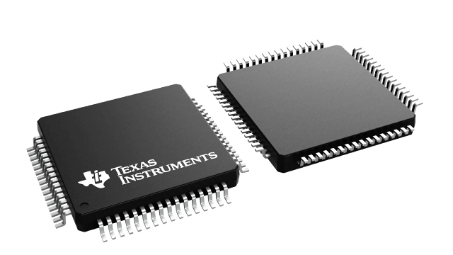
• Bus LVDS Signaling3.2 Nanosecond Propagation Delay MaxChip to Chip Skew ±800psLow Power CMOS DesignHigh Signaling Rate Capability (Above 100 Mbps)0.1V to 2.3V Common Mode Range for VID= 200mV±100 mV Receiver SensitivitySupports Open and Terminated Failsafe on Port Pins3.3V OperationGlitch Free Power Up/Down (Driver & Receiver Disabled)Light Bus Loading (5 pF Typical) per Bus LVDS LoadDesigned for Double Termination ApplicationsBalanced Output ImpedanceProduct Offered in 64 Pin LQFP PackageHigh Impedance Bus Pins on Power off (VCC= 0V)Driver Channel to Channel Skew (Same Device) 230ps TypicalReceiver Channel to Channel Skew (Same Device) 370ps TypicalAll trademarks are the property of their respective owners.Bus LVDS Signaling3.2 Nanosecond Propagation Delay MaxChip to Chip Skew ±800psLow Power CMOS DesignHigh Signaling Rate Capability (Above 100 Mbps)0.1V to 2.3V Common Mode Range for VID= 200mV±100 mV Receiver SensitivitySupports Open and Terminated Failsafe on Port Pins3.3V OperationGlitch Free Power Up/Down (Driver & Receiver Disabled)Light Bus Loading (5 pF Typical) per Bus LVDS LoadDesigned for Double Termination ApplicationsBalanced Output ImpedanceProduct Offered in 64 Pin LQFP PackageHigh Impedance Bus Pins on Power off (VCC= 0V)Driver Channel to Channel Skew (Same Device) 230ps TypicalReceiver Channel to Channel Skew (Same Device) 370ps TypicalAll trademarks are the property of their respective owners.
Description
AI
The DS92LV090A is one in a series of Bus LVDS transceivers designed specifically for the high speed, low power proprietary backplane or cable interfaces. The device operates from a single 3.3V power supply and includes nine differential line drivers and nine receivers. To minimize bus loading, the driver outputs and receiver inputs are internally connected. The separate I/O of the logic side allows for loop back support. The device also features a flow through pin out which allows easy PCB routing for short stubs between its pins and the connector.
The driver translates 3V TTL levels (single-ended) to differential Bus LVDS (BLVDS) output levels. This allows for high speed operation, while consuming minimal power with reduced EMI. In addition, the differential signaling provides common mode noise rejection of ±1V.
The receiver threshold is less than ±100 mV over a ±1V common mode range and translates the differential Bus LVDS to standard (TTL/CMOS) levels. (See Section for more details.)


