Catalog
2 A, Low VIN, Low Noise, CMOS Linear Regulator
Key Features
• 2 A maximum output current
• Low input voltage supply rangeVIN= 1.10 V to 1.98 V, no external bias supply required
• VIN= 1.10 V to 1.98 V, no external bias supply required
• Fixed output voltage range: VOUT_FIXED= 0.9 V to 1.5 V
• Adjustable output voltage range: VOUT_ADJ= 0.5 V to 1.5 V
• Ultralow noise: 2 μV rms, 100 Hz to 100 kHz
• Noise spectral density4 nV/√Hz at 10 kHz3 nV/√Hzat 100 kHz
• 4 nV/√Hz at 10 kHz
• 3 nV/√Hzat 100 kHz
• Low dropout voltage: 62 mV typical at 2 A load
• Operating supply current: 4.5 mA typical at no load
• ±1.5% fixed output voltage accuracy over line, load, and temperature
• Excellent power supply rejection ratio (PSRR) performance62 dB typical at 10 kHz at 2 A load46 dB typical at 100 kHz at 2 A load
• 62 dB typical at 10 kHz at 2 A load
• 46 dB typical at 100 kHz at 2 A load
• Excellent load/line transient response
• Soft start to reduce inrush current
• Optimized for small 10 μF ceramic capacitors
• Current-limit and thermal overload protection
• Power-good indicator
• Precision enable
• 16-lead, 3 mm × 3 mm LFCSP package
• AEC-Q100 qualified for automotive applications
Description
AI
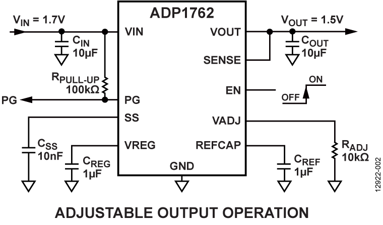
The ADP1762 is a low noise, low dropout (LDO) linear regulator. It is designed to operate from a single input supply with an input voltage as low as 1.10 V, without the requirement of an external bias supply, to increase efficiency and provide up to 2 A of output current.The low 62 mV typical dropout voltage at a 2 A load allows the ADP1762 to operate with a small headroom while maintaining regulation and providing better efficiency.The ADP1762 is optimized for stable operation with small 10 μF ceramic output capacitors. The ADP1762 delivers optimal transient performance with minimal board area.The ADP1762 is available in fixed output voltages ranging from 0.9 V to 1.5 V. The output of the adjustable output model can be set from 0.5 V to 1.5 V through an external resistor connected between VADJ and ground.The ADP1762 has an externally programmable soft start time by connecting a capacitor to the SS pin. Short-circuit and thermal overload protection circuits prevent damage in adverse conditions. The ADP1762 is available in a small 16-lead LFCSP package for the smallest footprint solution to meet a variety of applications.APPLICATIONSRegulation to noise sensitive applications such as radio frequency (RF) transceivers, analog-to-digital converter (ADC) and digital-to-analog converter (DAC) circuits, phase-locked loops (PLLs), voltage controlled oscillators (VCOs) and clocking integrated circuitsField-programmable gate array (FPGA) and digital signal processor (DSP) suppliesMedical and healthcareIndustrial and instrumentation


