AD4112 Series
Single Supply, 24-Bit, Sigma-Delta ADC with ±10 V and 0 mA to 20 mA Inputs
Manufacturer: Analog Devices
Catalog
Single Supply, 24-Bit, Sigma-Delta ADC with ±10 V and 0 mA to 20 mA Inputs
Key Features
• Internal or external clock
• Tested for robustness per: IEC61000-4-2, IEC61000-4-3, IEC61000-4-4, IEC61000-4-5, IEC61000-4-6, CISPR 11
• 24-bit ADC with integrated analog front endFast and flexible output rate: 1.25 SPS to 31.25 kSPSChannel scan data rate of 6.21 kSPS per channel (161 μs settling)16 noise free bits at 1 kSPS per channel85 dB rejection of 50 Hz and 60 Hz at 20 SPS per channel
• Fast and flexible output rate: 1.25 SPS to 31.25 kSPS
• Channel scan data rate of 6.21 kSPS per channel (161 μs settling)
• 16 noise free bits at 1 kSPS per channel
• 85 dB rejection of 50 Hz and 60 Hz at 20 SPS per channel
• ±10 V inputs, 4 differential or 8 single-endedPin absolute maximum rating ±50 VAbsolute input pin voltage up to ±20 V≥1 MΩ impedance±0.06% accuracy at 25°C
• Pin absolute maximum rating ±50 V
• Absolute input pin voltage up to ±20 V
• ≥1 MΩ impedance
• ±0.06% accuracy at 25°C
• 0 mA to 20 mA inputs, 4 single-endedPin absolute maximum rating ±50 mAInput range from −0.5 mA to +24 mA60 Ω impedance±0.08% accuracy at 25°C
• Pin absolute maximum rating ±50 mA
• Input range from −0.5 mA to +24 mA
• 60 Ω impedance
• ±0.08% accuracy at 25°C
• On-chip 2.5 V reference±0.12% accuracy at 25°C, ±5 ppm/°C (typical) drift
• ±0.12% accuracy at 25°C, ±5 ppm/°C (typical) drift
• Power suppliesAVDD = 3.0 V to 5.5 VIOVDD = 2 V to 5.5 VTotal IDD = 3.9 mA
• AVDD = 3.0 V to 5.5 V
• IOVDD = 2 V to 5.5 V
• Total IDD = 3.9 mA
• Temperature range: −40°C to +105°C
• 3-wire or 4-wire serial digital interface (Schmitt trigger on SCLK)SPI, QSPI, MICROWIRE, and DSP compatible
• SPI, QSPI, MICROWIRE, and DSP compatible
Description
AI
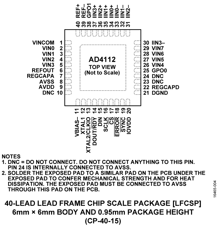
The AD4112 is a low power, low noise, 24-bit, sigma-delta (Σ-Δ) analog-to-digital converter (ADC) that integrates an analog front end (AFE) for fully differential or single-ended, high impedance (≥1 MΩ) bipolar, ±10 V voltage inputs, and 0 mA to 20 mA current inputs.The AD4112 also integrates key analog and digital signal conditioning blocks to configure eight individual setups for each analog input channel in use. The AD4112 features a maximum channel scan rate of 6.21 kSPS (161 µs) for fully settled data.The embedded 2.5 V, low drift (5 ppm/°C), band gap internal reference (with output reference buffer) reduces the external component count.The digital filter allows flexible settings, including simultaneous 50 Hz and 60 Hz rejection at a 27.27 SPS output data rate. The user can select between the different filter settings depending on the demands of each channel in the application. The automatic channel sequencer enables the ADC to switch through each enabled channel.The precision performance of the AD4112 is achieved by integrating the proprietaryiPassives™technology from Analog Devices, Inc. The AD4112 is factory calibrated to achieve a high degree of specified accuracy.The AD4112 operates with a single power supply, making it easy to use in galvanically isolated applications. The specified operating temperature range is −40°C to +105°C. The AD4112 is housed in a 40-lead, 6 mm × 6 mm LFCSP package.APPLICATIONSProcess controlPLC and DCS modulesInstrumentation and measurement


