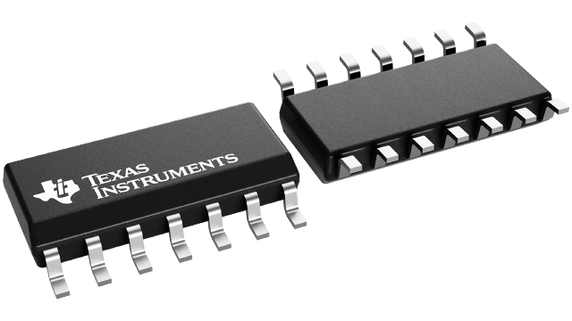
SN74HCS264-Q1 Series
Automotive 8-bit parallel-out serial shift registers
Manufacturer: Texas Instruments
Catalog
Automotive 8-bit parallel-out serial shift registers
Key Features
• AEC-Q100 Qualified for automotive applications:Device temperature grade 1: –40°C to +125°C, TADevice HBM ESD Classification Level 2Device CDM ESD Classifcation Level C6Wide operating voltage range: 2 V to 6 VSchmitt-trigger inputs allow for slow or noisy input signalsLow power consumptionTypical ICCof 100 nATypical input leakage current of ±100 nA7.8-mA output drive at 6 VAEC-Q100 Qualified for automotive applications:Device temperature grade 1: –40°C to +125°C, TADevice HBM ESD Classification Level 2Device CDM ESD Classifcation Level C6Wide operating voltage range: 2 V to 6 VSchmitt-trigger inputs allow for slow or noisy input signalsLow power consumptionTypical ICCof 100 nATypical input leakage current of ±100 nA7.8-mA output drive at 6 V
Description
AI
The SN74HCS264 device contains an 8-bit shift register with AND-gated serial inputs and an asynchronous clear (CLR) input. Data at the serial inputs can be changed while CLK is high or low, provided the minimum setup time requirements are met. All inputs include Schmitt-trigger architecture, adding noise margin and eliminating any input transition rate requirement. Clocking occurs on the low-to-high-level transition of CLK.
Upon a clock trigger, the device will store the result of the (A ● B) input data line in the first register and propagate each register’s data to the next register. The outputs are inverted from the data stored.


