Catalog
Precision 16-Bit, Buffered Voltage-Output DAC
Key Features
• 16-bit DAC with a two-buffer SPI interfaceAsynchronous load DAC and reset pinsCompatibility with 1.8V controllersBuffered voltage output with rail-to-rail capabilityWide voltage reference range of +2.5V to VAWide temperature range of −40°C to +105°CPackaged in a 16-pin LLP16-bit DAC with a two-buffer SPI interfaceAsynchronous load DAC and reset pinsCompatibility with 1.8V controllersBuffered voltage output with rail-to-rail capabilityWide voltage reference range of +2.5V to VAWide temperature range of −40°C to +105°CPackaged in a 16-pin LLP
Description
AI
The DAC161S055 is a precision 16-bit, buffered voltage output Digital-to-Analog Converter (DAC) that operates from a 2.7V to 5.25V supply with a separate I/O supply pin that operates down to 1.7V. The on-chip precision output buffer provides rail-to-rail output swing and has a typical settling time of 5 µsec. The external voltage reference can be set between 2.5V and VA(the analog supply voltage), providing the widest dynamic output range possible.
The 4-wire SPI compatible interface operates at clock rates up to 20 MHz. The part is capable of Diasy Chain and Data Read Back. An on board power-on-reset (POR) circuit ensures the output powers up to a known state.
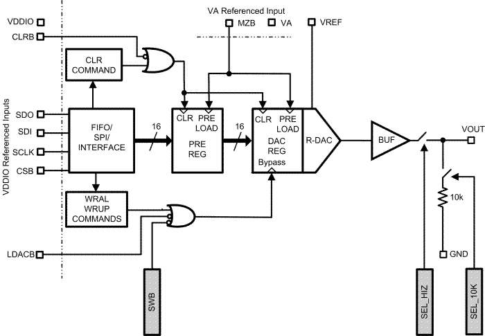
The DAC161S055 features a power-up value pin (MZB), a load DAC pin (LDACB) and a DAC clear (CLRB) pin. MZB sets the startup output voltage to either GND or mid-scale. LDACB updates the output, allowing multiple DACs to update their outputs simultaneously. CLRB can be used to reset the output signal to the value determined by MZB.
The DAC161S055 has a power-down option that reduces power consumption when the part is not in use. It is available in a 16-lead LLP package.


