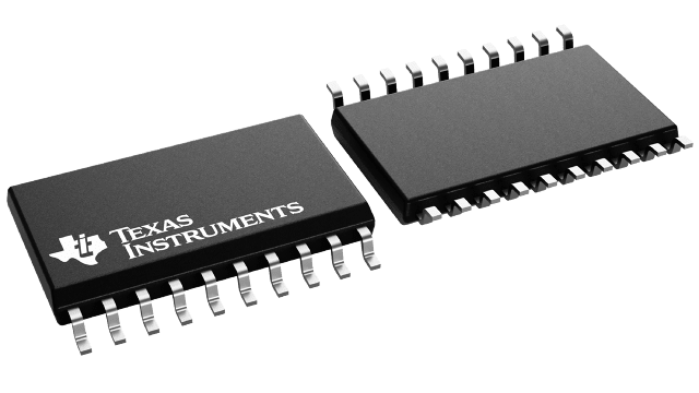
SN74LVCZ240A Series
8-ch, 2.7-V to 3.6-V inverters with 3-state outputs
Manufacturer: Texas Instruments
Catalog
8-ch, 2.7-V to 3.6-V inverters with 3-state outputs
| Part | Logic Type | Number of Bits per Element | Package / Case [y] | Package / Case | Package / Case [x] | Number of Elements | Output Type | Voltage - Supply [Min] | Voltage - Supply [Max] | Supplier Device Package | Mounting Type | Current - Output High, Low | Operating Temperature [Max] | Operating Temperature [Min] | Package / Case | Package / Case | Package / Case [y] |
|---|---|---|---|---|---|---|---|---|---|---|---|---|---|---|---|---|---|
Texas Instruments | Buffer Inverting | 4 | 4.4 mm | 20-TSSOP | 0.173 in | 2 | 3-State | 2.7 V | 3.6 V | 20-TSSOP | Surface Mount | 24 mA | 85 °C | -40 °C | |||
Texas Instruments | Buffer Inverting | 4 | 20-DIP | 2 | 3-State | 2.7 V | 3.6 V | 20-PDIP | Through Hole | 24 mA | 85 °C | -40 °C | 7.62 mm | 0.3 in | |||
Texas Instruments | Buffer Inverting | 4 | 20-SOIC | 2 | 3-State | 2.7 V | 3.6 V | 20-SO | Surface Mount | 24 mA | 85 °C | -40 °C | 5.3 mm | 0.209 " | |||
Texas Instruments | Buffer Inverting | 4 | 0.295 in | 20-SOIC | 2 | 3-State | 2.7 V | 3.6 V | 20-SOIC | Surface Mount | 24 mA | 85 °C | -40 °C | 7.5 mm | |||
Texas Instruments | Buffer Inverting | 4 | 4.4 mm | 20-TSSOP | 0.173 in | 2 | 3-State | 2.7 V | 3.6 V | 20-TSSOP | Surface Mount | 24 mA | 85 °C | -40 °C | |||
Texas Instruments | Buffer Inverting | 4 | 0.173 in | 20-TFSOP | 2 | 3-State | 2.7 V | 3.6 V | 20-TVSOP | Surface Mount | 24 mA | 85 °C | -40 °C | 4.4 mm |
Key Features
• Operates From 2.7 V to 3.6 VInputs Accept Voltages to 5.5 VMax tpdof 6.5 ns at 3.3 VTypical VOLP(Output Ground Bounce)<0.8 V at VCC= 3.3 V, TA= 25°CTypical VOHV(Output VOHUndershoot)<2 V at VCC= 3.3 V, TA= 25°CIoffand Power-Up 3-State Support Hot InsertionSupports Mixed-Mode Signal Operation on All Ports (5-V Input/Output Voltage With 3.3-V VCC)Latch-Up Performance Exceeds 100 mA Per JESD 78, Class IIESD Protection Exceeds JESD 222000-V Human-Body Model (A114-A)200-V Machine Model (A115-A)1000-V Charged-Device Model (C101)Operates From 2.7 V to 3.6 VInputs Accept Voltages to 5.5 VMax tpdof 6.5 ns at 3.3 VTypical VOLP(Output Ground Bounce)<0.8 V at VCC= 3.3 V, TA= 25°CTypical VOHV(Output VOHUndershoot)<2 V at VCC= 3.3 V, TA= 25°CIoffand Power-Up 3-State Support Hot InsertionSupports Mixed-Mode Signal Operation on All Ports (5-V Input/Output Voltage With 3.3-V VCC)Latch-Up Performance Exceeds 100 mA Per JESD 78, Class IIESD Protection Exceeds JESD 222000-V Human-Body Model (A114-A)200-V Machine Model (A115-A)1000-V Charged-Device Model (C101)
Description
AI
This octal buffer/driver is designed for 2.7-V to 3.6-V VCCoperation.
The SN74LVCZ240A is designed specifically to improve the performance and density of 3-state memory address drivers, clock drivers, and bus-oriented receivers and transmitters.
This device is organized as two 4-bit buffers/drivers with separate output-enable (OE)\ inputs. When OE\ is low, the device passes data from the A inputs to the Y outputs. When OE\ is high, the outputs are in the high-impedance state.
Inputs can be driven from either 3.3-V or 5-V devices. This feature allows the use of this device as a translator in a mixed 3.3-V/5-V system environment.
When VCCis between 0 and 1.5 V, the device is in the high-impedance state during power up or power down. However, to ensure the high-impedance state above 1.5 V, OE\ should be tied to VCCthrough a pullup resistor; the minimum value of the resistor is determined by the current-sinking capability of the driver.
This device is fully specified for hot-insertion applications using Ioffand power-up 3-state. The Ioffcircuitry disables the outputs, preventing damaging current backflow through the device when it is powered down. The power-up 3-state circuitry places the outputs in the high-impedance state during power up and power down, which prevents driver conflict.


