THS10064 Series
10-Bit, 6 MSPS ADC Quad Ch. (Config.), DSP/uP Interface, Integ. 16x FIFO, Ch. AutoScan, Low Power
Manufacturer: Texas Instruments
Catalog
10-Bit, 6 MSPS ADC Quad Ch. (Config.), DSP/uP Interface, Integ. 16x FIFO, Ch. AutoScan, Low Power
Key Features
• High-Speed 6 MSPS ADC4 Analog InputsSimultaneous Sampling of 4 Single-Ended Signals or 2 Differential Signals or Combination of BothDifferential Nonlinearity Error: ±1 LSBIntegral Nonlinearity Error: ±1.5 LSBSignal-to-Noise and Distortion Ratio: 59 dB at fI= 2 MHzAuto-Scan Mode for 2, 3, or 4 Inputs3-V or 5-V Digital Interface CompatibleLow Power: 216 mW Max5-V Analog Single Supply OperationInternal Voltage References ...50 PPM/°C and ±5% AccuracyGlueless DSP InterfaceParallel µC/DSP InterfaceIntegrated FIFOAvailable in TSSOP PackagePin Compatible With 12-Bit THS1206APPLICATIONSRadar ApplicationsCommunicationsControl ApplicationsHigh-Speed DSP Front-EndAutomotive ApplicationsHigh-Speed 6 MSPS ADC4 Analog InputsSimultaneous Sampling of 4 Single-Ended Signals or 2 Differential Signals or Combination of BothDifferential Nonlinearity Error: ±1 LSBIntegral Nonlinearity Error: ±1.5 LSBSignal-to-Noise and Distortion Ratio: 59 dB at fI= 2 MHzAuto-Scan Mode for 2, 3, or 4 Inputs3-V or 5-V Digital Interface CompatibleLow Power: 216 mW Max5-V Analog Single Supply OperationInternal Voltage References ...50 PPM/°C and ±5% AccuracyGlueless DSP InterfaceParallel µC/DSP InterfaceIntegrated FIFOAvailable in TSSOP PackagePin Compatible With 12-Bit THS1206APPLICATIONSRadar ApplicationsCommunicationsControl ApplicationsHigh-Speed DSP Front-EndAutomotive Applications
Description
AI
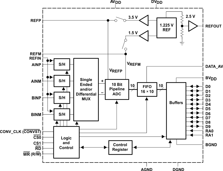
The THS10064 is a CMOS, low-power, 10-bit, 6 MSPS analog-to-digital converter (ADC). The speed, resolution, bandwidth, and single-supply operation are suited for applications in radar, imaging, high-speed acquisition, and communications. A multistage pipelined architecture with output error correction logic provides for no missing codes over the full operating temperature range. Internal control registers are used to program the ADC into the desired mode. The THS10064 consists of four analog inputs, which are sampled simultaneously. These inputs can be selected individually and configured to single-ended or differential inputs. An integrated 16 word deep FIFO allows the storage of data in order to improve data transfers to the processor. Internal reference voltages for the ADC (1.5 V and 3.5 V) are provided.
An external reference can also be chosen to suit the dc accuracy and temperature drift requirements of the application. Two different conversion modes can be selected. In single conversion mode, a single and simultaneous conversion of up to four inputs can be initiated by using the single conversion start signal (CONVST)\. The conversion clock in single conversion mode is generated internally using a clock oscillator circuit. In continuous conversion mode, an external clock signal is applied to the CONV_CLK input of the THS10064. The internal clock oscillator is switched off in continuous conversion mode.
The THS10064C is characterized for operation from 0°C to 70°C, and the THS10064I is characterized for operation from –40°C to 85°C.


