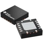
TPS54620RGYT
ActiveCONV DC-DC 4.5V TO 17V SYNCHRONOUS STEP DOWN SINGLE-OUT 0.8V TO 15V 6A 14-PIN VQFN EP T/R
Deep-Dive with AI
Search across all available documentation for this part.

TPS54620RGYT
ActiveCONV DC-DC 4.5V TO 17V SYNCHRONOUS STEP DOWN SINGLE-OUT 0.8V TO 15V 6A 14-PIN VQFN EP T/R
Technical Specifications
Parameters and characteristics for this part
| Specification | TPS54620RGYT |
|---|---|
| Current - Output | 6 A |
| Frequency - Switching [Max] | 1.6 MHz |
| Frequency - Switching [Min] | 200 kHz |
| Function | Step-Down |
| Mounting Type | Surface Mount |
| Number of Outputs | 1 |
| Operating Temperature [Max] | 150 °C |
| Operating Temperature [Min] | -40 °C |
| Output Configuration | Positive |
| Output Type | Adjustable |
| Package / Case | 14-VFQFN Exposed Pad |
| Supplier Device Package | 3.5x3.5, 14-VQFN |
| Synchronous Rectifier | True |
| Topology | Buck |
| Voltage - Input (Max) [Max] | 17 V |
| Voltage - Input (Min) [Min] | 4.5 V |
| Voltage - Output (Max) [Max] | 15 V |
| Voltage - Output (Min/Fixed) | 0.8 V |
Pricing
Prices provided here are for design reference only. For realtime values and availability, please visit the distributors directly
| Distributor | Package | Quantity | $ | |
|---|---|---|---|---|
| Digikey | Cut Tape (CT) | 1 | $ 6.63 | |
| 10 | $ 5.95 | |||
| 25 | $ 5.63 | |||
| 100 | $ 4.88 | |||
| Digi-Reel® | 1 | $ 6.63 | ||
| 10 | $ 5.95 | |||
| 25 | $ 5.63 | |||
| 100 | $ 4.88 | |||
| N/A | 2473 | $ 6.73 | ||
| Tape & Reel (TR) | 250 | $ 4.63 | ||
| 500 | $ 4.15 | |||
| 1250 | $ 3.50 | |||
| 2500 | $ 3.33 | |||
| Texas Instruments | SMALL T&R | 1 | $ 4.56 | |
| 100 | $ 3.72 | |||
| 250 | $ 2.92 | |||
| 1000 | $ 2.48 | |||
Description
General part information
TPS54620 Series
The TPS54620 in thermally enhanced 3.50 mm × 3.50 mm QFN package is a full featured 17-V, 6-A, synchronous, step-down converter which is optimized for small designs through high efficiency and integrating the high-side and low-side MOSFETs. Further space savings are achieved through current mode control, which reduces component count, and by selecting a high switching frequency, reducing the footprint of the inductor.
The output voltage start-up ramp is controlled by the SS/TR pin which allows operation as either a stand-alone power supply or in tracking situations. Power sequencing is also possible by correctly configuring the enable and the open-drain power good pins.
Cycle-by-cycle current limiting on the high-side FET protects the device in overload situations and is enhanced by a low-side sourcing current limit which prevents current runaway. There is also a low-side sinking current limit that turns off the low-side MOSFET to prevent excessive reverse current. Thermal shutdown disables the part when die temperature exceeds thermal shutdown temperature.
Documents
Technical documentation and resources


