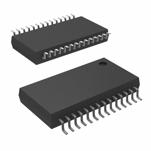
CDC319DB
Active1-LINE TO 10-LINE CLOCK DRIVER WITH I2C CONTROL INTERFACE
Deep-Dive with AI
Search across all available documentation for this part.

CDC319DB
Active1-LINE TO 10-LINE CLOCK DRIVER WITH I2C CONTROL INTERFACE
Deep-Dive with AI
Technical Specifications
Parameters and characteristics for this part
| Specification | CDC319DB |
|---|---|
| Differential - Input:Output | False |
| Frequency - Max [Max] | 100 MHz |
| Mounting Type | Surface Mount |
| Number of Circuits | 1 |
| Operating Temperature [Max] | 70 °C |
| Operating Temperature [Min] | 0 °C |
| Output | LVTTL, TTL |
| Package / Case | 28-SSOP |
| Package / Case [custom] | 0.209 in |
| Package / Case [custom] | 5.3 mm |
| Ratio - Input:Output [custom] | 1:10 |
| Supplier Device Package | 28-SSOP |
| Type | Fanout Buffer (Distribution), Data |
| Voltage - Supply [Max] | 3.465 V |
| Voltage - Supply [Min] | 3.135 V |
Pricing
Prices provided here are for design reference only. For realtime values and availability, please visit the distributors directly
| Distributor | Package | Quantity | $ | |
|---|---|---|---|---|
| Digikey | Tube | 150 | $ 8.23 | |
| Texas Instruments | TUBE | 1 | $ 9.25 | |
| 100 | $ 8.11 | |||
| 250 | $ 5.68 | |||
| 1000 | $ 4.58 | |||
Description
General part information
CDC319 Series
The CDC319 is a high-performance clock buffer that distributes one input (A) to 10 outputs (Y) with minimum skew for clock distribution. The CDC319 operates from a 3.3-V power supply, and is characterized for operation from 0°C to 70°C.
The device provides a standard mode (100K-bits/s) I2C serial interface for device control. The implementation is as a slave/receiver. The device address is specified in the I2C device address table. Both of the I2C inputs (SDATA and SCLOCK) provide integrated pullup resistors (typically 140 k) and are 5-V tolerant.
Three 8-bit I2C registers provide individual enable control for each of the outputs. All outputs default to enabled at powerup. Each output can be placed in a disabled mode with a low-level output when a low-level control bit is written to the control register. The registers are write only and must be accessed in sequential order (i.e., random access of the registers is not supported).
Documents
Technical documentation and resources


