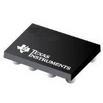
CDC3RL02YFPR
ActiveDUAL-CHANNEL SQUARE/SINE-TO-SQUARE WAVE CLOCK BUFFER
Deep-Dive with AI
Search across all available documentation for this part.

CDC3RL02YFPR
ActiveDUAL-CHANNEL SQUARE/SINE-TO-SQUARE WAVE CLOCK BUFFER
Deep-Dive with AI
Technical Specifications
Parameters and characteristics for this part
| Specification | CDC3RL02YFPR |
|---|---|
| Differential - Input:Output | False |
| Frequency - Max [Max] | 52 MHz |
| Input | LVCMOS |
| Mounting Type | Surface Mount |
| Number of Circuits | 1 |
| Operating Temperature [Max] | 85 °C |
| Operating Temperature [Min] | -40 °C |
| Output | LVCMOS |
| Package / Case | 8-XFBGA, DSBGA |
| Ratio - Input:Output [custom] | 1:2 |
| Supplier Device Package | 8-DSBGA |
| Type | Fanout Buffer (Distribution) |
| Voltage - Supply [Max] | 5.5 V |
| Voltage - Supply [Min] | 2.3 V |
Pricing
Prices provided here are for design reference only. For realtime values and availability, please visit the distributors directly
| Distributor | Package | Quantity | $ | |
|---|---|---|---|---|
| Arrow | N/A | 1 | $ 1.46 | |
| 10 | $ 0.98 | |||
| 50 | $ 0.98 | |||
| 100 | $ 0.87 | |||
| 200 | $ 0.81 | |||
| Digikey | Cut Tape (CT) | 1 | $ 1.63 | |
| 10 | $ 1.46 | |||
| 25 | $ 1.38 | |||
| 100 | $ 1.17 | |||
| 250 | $ 1.10 | |||
| 500 | $ 0.97 | |||
| 1000 | $ 0.80 | |||
| Digi-Reel® | 1 | $ 1.63 | ||
| 10 | $ 1.46 | |||
| 25 | $ 1.38 | |||
| 100 | $ 1.17 | |||
| 250 | $ 1.10 | |||
| 500 | $ 0.97 | |||
| 1000 | $ 0.80 | |||
| Tape & Reel (TR) | 3000 | $ 0.74 | ||
| 6000 | $ 0.72 | |||
| Texas Instruments | LARGE T&R | 1 | $ 1.17 | |
| 100 | $ 0.90 | |||
| 250 | $ 0.66 | |||
| 1000 | $ 0.47 | |||
Description
General part information
CDC3RL02 Series
The CDC3RL02 is a two-channel clock fan-out buffer and is designed for use in portable end-equipment, such as mobile phones, that require clock buffering with minimal additive phase noise and fan-out capabilities. The device buffers a single clock source, such as a temperature compensated crystal oscillator (TCXO) to multiple peripherals. The device has two clock request inputs (CLK_REQ1 and CLK_REQ2), each input can enable a single clock output.
The CDC3RL02 accepts square or sine waves at the master clock input (MCLK_IN), eliminating the need for an AC coupling capacitor. The smallest acceptable sine wave is a 0.3V signal (peak-to-peak). CDC3RL02 is designed to offer minimal channel-to-channel skew, additive output jitter, and additive phase noise. The adaptive clock output buffers offer controlled slew-rate over a wide capacitive loading range which minimizes EMI emissions, maintains signal integrity, and minimizes ringing caused by signal reflections on the clock distribution lines.
The CDC3RL02 has an integrated Low-Drop-Out (LDO) voltage regulator which accepts input voltages from 2.3V to 5.5V and outputs 1.8V, 50mA. This 1.8V supply is externally available to provide regulated power to peripheral devices such as a TCXO.
Documents
Technical documentation and resources


