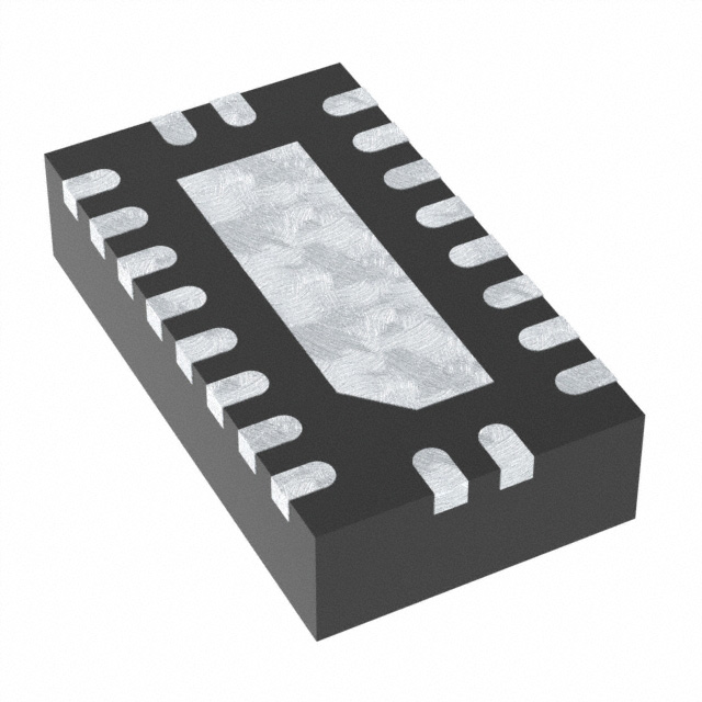
HD3SS3212IRKSR
Active2-CHANNEL 10-GBPS 2:1/1:2 USB 3.1 DIFFERENTIAL MUX/DEMUX
Deep-Dive with AI
Search across all available documentation for this part.

HD3SS3212IRKSR
Active2-CHANNEL 10-GBPS 2:1/1:2 USB 3.1 DIFFERENTIAL MUX/DEMUX
Technical Specifications
Parameters and characteristics for this part
| Specification | HD3SS3212IRKSR |
|---|---|
| -3db Bandwidth | 8 GHz |
| Applications | USB |
| Mounting Type | Surface Mount |
| Multiplexer/Demultiplexer Circuit | 2:1 |
| Number of Channels [custom] | 2 |
| On-State Resistance (Max) [Max] | 8 Ohm |
| Operating Temperature [Max] | 85 °C |
| Operating Temperature [Min] | -40 °C |
| Package / Case | 20-VFQFN Exposed Pad |
| Supplier Device Package | 20-VQFN (2.5x4.5) |
| Switch Circuit | SPDT |
| Voltage - Supply, Single (V+) [Max] | 3.6 V |
| Voltage - Supply, Single (V+) [Min] | 2.7 V |
Pricing
Prices provided here are for design reference only. For realtime values and availability, please visit the distributors directly
| Distributor | Package | Quantity | $ | |
|---|---|---|---|---|
| Digikey | Cut Tape (CT) | 1 | $ 1.67 | |
| 10 | $ 1.50 | |||
| 25 | $ 1.41 | |||
| 100 | $ 1.21 | |||
| 250 | $ 1.13 | |||
| 500 | $ 1.00 | |||
| Digi-Reel® | 1 | $ 1.67 | ||
| 10 | $ 1.50 | |||
| 25 | $ 1.41 | |||
| 100 | $ 1.21 | |||
| 250 | $ 1.13 | |||
| 500 | $ 1.00 | |||
| Tape & Reel (TR) | 3000 | $ 1.00 | ||
| Texas Instruments | LARGE T&R | 1 | $ 1.78 | |
| 100 | $ 1.47 | |||
| 250 | $ 1.06 | |||
| 1000 | $ 0.80 | |||
Description
General part information
HD3SS3212 Series
The HD3SS3212 is a high-speed bidirectional passive switch in mux or demux configurations suited for USB Type-C™ application supporting USB 3.1 Gen 1 and Gen 2 data rates. Based on control pin SEL, the device provides switching on differential channels between Port B or Port C to Port A.
The HD3SS3212 is a generic analog differential passive switch that can work for any high-speed interface applications requiring a common mode voltage range of 0 to 2 V and differential signaling with differential amplitude up to 1800 mVpp. It employs adaptive tracking that ensures the channel remains unchanged for the entire common mode voltage range.
Excellent dynamic characteristics of the device allow high-speed switching with minimum attenuation to the signal eye diagram with very little added jitter. It consumes <2 mW of power when operational and has a shutdown mode exercisable by OEn pin resulting <20 µW.
Documents
Technical documentation and resources


