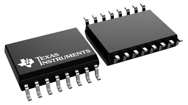
CY74FCT399ATSOCT
ActiveQUADRUPLE 2-INPUT MULTIPLEXERS WITH STORAGE
Deep-Dive with AI
Search across all available documentation for this part.

CY74FCT399ATSOCT
ActiveQUADRUPLE 2-INPUT MULTIPLEXERS WITH STORAGE
Deep-Dive with AI
Technical Specifications
Parameters and characteristics for this part
| Specification | CY74FCT399ATSOCT |
|---|---|
| Circuit | 4 x 1:1 |
| Current - Output High, Low [custom] | 64 mA |
| Current - Output High, Low [custom] | 32 mA |
| Independent Circuits | 1 |
| Mounting Type | Surface Mount |
| Operating Temperature [Max] | 85 °C |
| Operating Temperature [Min] | -40 °C |
| Package / Case | 16-SOIC |
| Package / Case [x] | 0.295 in |
| Package / Case [y] | 7.5 mm |
| Supplier Device Package | 16-SOIC |
| Type | Multiplexer |
| Voltage - Supply [Max] | 5.25 V |
| Voltage - Supply [Min] | 4.75 V |
| Voltage Supply Source | Single Supply |
Pricing
Prices provided here are for design reference only. For realtime values and availability, please visit the distributors directly
| Distributor | Package | Quantity | $ | |
|---|---|---|---|---|
| Digikey | Tape & Reel (TR) | 2000 | $ 0.80 | |
| 6000 | $ 0.77 | |||
| 10000 | $ 0.74 | |||
| Texas Instruments | LARGE T&R | 1 | $ 1.32 | |
| 100 | $ 1.09 | |||
| 250 | $ 0.78 | |||
| 1000 | $ 0.59 | |||
Description
General part information
CY74FCT399T Series
The CY74FCT399T is a high-speed quad 2-input register that selects four bits of data from either of two sources (ports) under control of a common select (S) input. Selected data are transferred to a 4-bit output register synchronous with the low-to-high transition of the clock (CP) input. The 4-bit D-type output register is fully edge triggered. The data inputs (I0X, I1X) and S input must be stable only one setup time prior to, and hold time after, the low-to-high transition of CP for predictable operation. The CY74FCT399T has noninverted outputs.
This device is fully specified for partial-power-down applications using IoffThe Ioffcircuitry disables the outputs, preventing damaging current backflow through the device when it is powered down.
The CY74FCT399T is a high-speed quad 2-input register that selects four bits of data from either of two sources (ports) under control of a common select (S) input. Selected data are transferred to a 4-bit output register synchronous with the low-to-high transition of the clock (CP) input. The 4-bit D-type output register is fully edge triggered. The data inputs (I0X, I1X) and S input must be stable only one setup time prior to, and hold time after, the low-to-high transition of CP for predictable operation. The CY74FCT399T has noninverted outputs.
Documents
Technical documentation and resources


