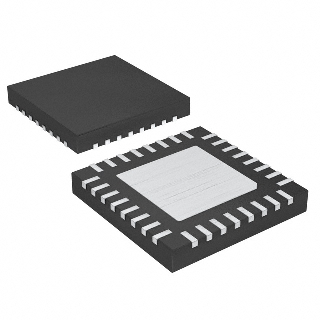
MC100EP809MNG
ActiveCLOCK BUFFER, DRIVER, FANOUT, 100 MHZ TO 750 MHZ, 9 OUTPUTS, 3 V TO 3.6 V, 32 PINS, QFN-EP

MC100EP809MNG
ActiveCLOCK BUFFER, DRIVER, FANOUT, 100 MHZ TO 750 MHZ, 9 OUTPUTS, 3 V TO 3.6 V, 32 PINS, QFN-EP
Technical Specifications
Parameters and characteristics for this part
| Specification | MC100EP809MNG |
|---|---|
| Differential - Input:Output [custom] | True |
| Differential - Input:Output [custom] | True |
| Frequency - Max [Max] | 750 MHz |
| Input | LVDS, LVPECL, HSTL |
| Mounting Type | Surface Mount |
| Number of Circuits | 2 |
| Operating Temperature [Max] | 85 °C |
| Operating Temperature [Min] | 0 °C |
| Output | HSTL |
| Package / Case | 32-VFQFN Exposed Pad |
| Ratio - Input:Output | 1:9 |
| Supplier Device Package | 32-QFN (5x5) |
| Type | Fanout Buffer (Distribution), Multiplexer |
| Voltage - Supply [Max] | 3.6 V |
| Voltage - Supply [Min] | 3 V |
Pricing
Prices provided here are for design reference only. For realtime values and availability, please visit the distributors directly
Description
General part information
MC100EP809 Series
The MC100EP809 is a low skew 2:1:9 differential bus clock driver, designed with clock distribution in mind, accepting two clock sources into an input multiplexer. The part is designed for use in low voltage applications which require a large number of outputs to drive precisely aligned low skew signals to their destination. The two clock inputs are one differential HSTL and one differential LVPECL. Both input pairs can accept LVDS levels. They are selected by the CLK_SEL pin which is LVTTL. To avoid generation of a runt clock pulse when the device is enabled/disabled, the Output Enable (OE), which is LVTTL, is synchronous so that the outputs will only be enabled/disabled when they are already in LOW state.The MC100EP809 guarantees low output-to-output skew. The optimal design, layout, and processing minimize skew within a device and from lot to lot. The MC100EP809 output structure uses open emitter architecture and will be terminated with 50 to ground instead of a standard HSTL configuration. To ensure that tight skew specification is realized, both sides of the differential output need to be terminated identically into 50 even if only one output is being used. If an output pair is unused, both outputs may be left open (unterminated) without affecting skew.Designers can take advantage of the EP809's performance to distribute low skew clocks across the backplane of the board. HSTL clock inputs may be driven single-end by biasing the non-driven pin in an input pair.
Documents
Technical documentation and resources


