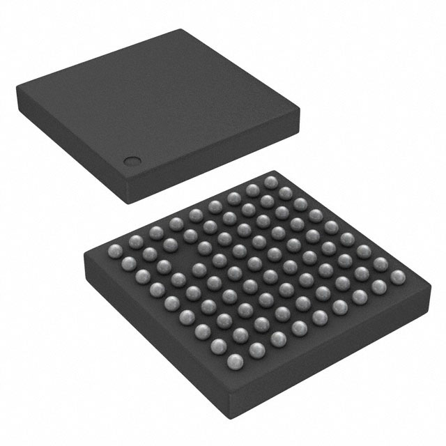
SN65LVDS301ZXH
ActivePROGRAMMABLE 27-BIT DISPLAY SERIAL INTERFACE TRANSMITTER
Deep-Dive with AI
Search across all available documentation for this part.

SN65LVDS301ZXH
ActivePROGRAMMABLE 27-BIT DISPLAY SERIAL INTERFACE TRANSMITTER
Deep-Dive with AI
Technical Specifications
Parameters and characteristics for this part
| Specification | SN65LVDS301ZXH |
|---|---|
| Data Rate | 1.755 Gbps |
| Function | Serializer |
| Input Type | CMOS |
| Mounting Type | Surface Mount |
| Number of Inputs | 24 |
| Number of Outputs | 3 |
| Operating Temperature [Max] | 85 °C |
| Operating Temperature [Min] | -40 °C |
| Output Type | LVDS |
| Package / Case | 80-VFBGA |
| Supplier Device Package | 80-NFBGA (5x5) |
| Voltage - Supply [Max] | 1.95 V |
| Voltage - Supply [Min] | 1.65 V |
Pricing
Prices provided here are for design reference only. For realtime values and availability, please visit the distributors directly
| Distributor | Package | Quantity | $ | |
|---|---|---|---|---|
| Digikey | Tray | 1 | $ 3.87 | |
| 10 | $ 3.48 | |||
| 25 | $ 3.29 | |||
| 80 | $ 2.85 | |||
| 230 | $ 2.70 | |||
| 576 | $ 2.57 | |||
| Texas Instruments | JEDEC TRAY (5+1) | 1 | $ 4.16 | |
| 100 | $ 3.64 | |||
| 250 | $ 2.56 | |||
| 1000 | $ 2.06 | |||
Description
General part information
SN65LVDS301 Series
The SN65LVDS301 serializer device converts 27 parallel data inputs to 1, 2, or 3 Sub Low-Voltage Differential Signaling (SubLVDS) serial outputs. It loads a shift register with 24 pixel bits and 3 control bits from the parallel CMOS input interface. In addition to the 27 data bits, the device adds a parity bit and two reserved bits into a 30-bit data word. Each word is latched into the device by the pixel clock (PCLK). The parity bit (odd parity) allows a receiver to detect single bit errors. The serial shift register is uploaded at 30, 15, or 10 times the pixel-clock data rate depending on the number of serial links used. A copy of the pixel clock is output on a separate differential output.
FPC cabling typically interconnects the SN65LVDS301 with the display. Compared to parallel signaling, the LVDS301 outputs significantly reduce the EMI of the interconnect by over 20 dB. The electromagnetic emission of the device itself is very low and meets the meets SAE J1752/3 ’M’-spec. (see Figure 6-22)
The SN65LVDS301 is characterized for operation over ambient air temperatures of –40°C to 85°C. All CMOS inputs offer failsafe features to protect them from damage during power-up and to avoid current flow into the device inputs during power-up. An input voltage of up to 2.165 V can be applied to all CMOS inputs while VDDis between 0V and 1.65V.
Documents
Technical documentation and resources


