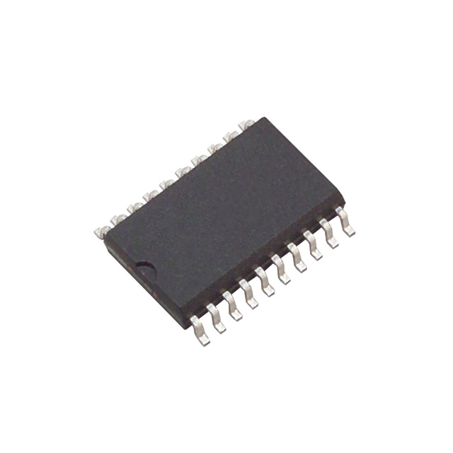
SN74AS757DWR
ActiveBUFFER/LINE DRIVER 8-CH NON-INVERTING 3-ST/OPEN COLLECTOR BIPOLAR 20-PIN SOIC T/R
Deep-Dive with AI
Search across all available documentation for this part.

SN74AS757DWR
ActiveBUFFER/LINE DRIVER 8-CH NON-INVERTING 3-ST/OPEN COLLECTOR BIPOLAR 20-PIN SOIC T/R
Deep-Dive with AI
Technical Specifications
Parameters and characteristics for this part
| Specification | SN74AS757DWR |
|---|---|
| Current - Output High, Low [custom] | - |
| Current - Output High, Low [custom] | 64 mA |
| Logic Type | Buffer, Non-Inverting |
| Mounting Type | Surface Mount |
| Number of Bits per Element | 4 |
| Number of Elements | 2 |
| Operating Temperature [Max] | 70 °C |
| Operating Temperature [Min] | 0 °C |
| Output Type | Open Collector |
| Package / Case | 20-SOIC |
| Package / Case [y] | 0.295 in |
| Package / Case [y] | 7.5 mm |
| Supplier Device Package | 20-SOIC |
| Voltage - Supply [Max] | 5.5 V |
| Voltage - Supply [Min] | 4.5 V |
Pricing
Prices provided here are for design reference only. For realtime values and availability, please visit the distributors directly
| Distributor | Package | Quantity | $ | |
|---|---|---|---|---|
| Digikey | Tape & Reel (TR) | 2000 | $ 6.06 | |
| Texas Instruments | LARGE T&R | 1 | $ 8.80 | |
| 100 | $ 7.69 | |||
| 250 | $ 5.93 | |||
| 1000 | $ 5.30 | |||
Description
General part information
SN74AS757 Series
These octal buffers and line drivers are designed specifically to improve the performance and density of 3-state memory address drivers, clock drivers, and bus-oriented receivers and transmitters by eliminating the need for 3-state overlap protection. The designer has a choice of selected combinations of inverting and noninverting outputs, symmetrical active-low output-enable () inputs, and complementary OE andinputs. These devices feature high fan-out and improved fan-in.
The SN54AS756 is characterized for operation over the full military temperature range of -55°C to 125°C. The SN74AS756 and SN74AS757 are characterized for operation from 0°C to 70°C.
These octal buffers and line drivers are designed specifically to improve the performance and density of 3-state memory address drivers, clock drivers, and bus-oriented receivers and transmitters by eliminating the need for 3-state overlap protection. The designer has a choice of selected combinations of inverting and noninverting outputs, symmetrical active-low output-enable () inputs, and complementary OE andinputs. These devices feature high fan-out and improved fan-in.
Documents
Technical documentation and resources


