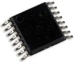
NLVLVX4052DTR2G
ObsoleteANALOG MULTIPLEXER/DEMULTIPLEXER, 2 CIRCUITS, 4:1, 86 OHM, 2.5V TO 6V, TSSOP-16, -55 °C TO 125 °C
Deep-Dive with AI
Search across all available documentation for this part.

NLVLVX4052DTR2G
ObsoleteANALOG MULTIPLEXER/DEMULTIPLEXER, 2 CIRCUITS, 4:1, 86 OHM, 2.5V TO 6V, TSSOP-16, -55 °C TO 125 °C
Deep-Dive with AI
Technical Specifications
Parameters and characteristics for this part
| Specification | NLVLVX4052DTR2G |
|---|---|
| -3db Bandwidth | 80 MHz |
| Channel Capacitance (CS(off), CD(off)) [custom] | 10 pF |
| Channel Capacitance (CS(off), CD(off)) [custom] | 10 pF |
| Channel-to-Channel Matching (ΔRon) | 10 Ohm |
| Charge Injection | 12 pC |
| Current - Leakage (IS(off)) (Max) [Max] | 100 nA |
| Grade | Automotive |
| Multiplexer/Demultiplexer Circuit | 4:1 |
| Number of Circuits | 2 |
| On-State Resistance (Max) [Max] | 26 Ohm |
| Operating Temperature [Max] | 125 °C |
| Operating Temperature [Min] | -55 °C |
| Qualification | AEC-Q100 |
| Switch Circuit | SP4T |
| Voltage - Supply, Dual (V±) | 6 V |
| Voltage - Supply, Dual (V±) [Max] | 2.5 V |
| Voltage - Supply, Dual (V±) [Min] | -2.5 V |
| Voltage - Supply, Single (V+) [Max] | 6 V |
| Voltage - Supply, Single (V+) [Min] | 2.5 V |
Pricing
Prices provided here are for design reference only. For realtime values and availability, please visit the distributors directly
| Distributor | Package | Quantity | $ | |
|---|---|---|---|---|
| Newark | Each (Supplied on Full Reel) | 1 | $ 0.40 | |
| 3000 | $ 0.39 | |||
| 6000 | $ 0.36 | |||
| 12000 | $ 0.34 | |||
| 18000 | $ 0.31 | |||
| 30000 | $ 0.30 | |||
Description
General part information
MC74LVX4052 Series
The MC74LVX4052 utilizes silicon-gate CMOS technology to achieve fast propagation delays, low ON resistances, and low OFF leakage currents. This analog multiplexer/demultiplexer controls analog voltages that may vary across the complete power supply range (from VCCto VEE).The LVX4052 is similar in pinout to the high-speed HC4052A, and the metal-gate MC14052B. The Channel-Select inputs determine which one of the Analog Inputs/Outputs is to be connected, by means of an analog switch, to the Common Output/Input. When the Enable pin is HIGH, all analog switches are turned off.The Channel-Select and Enable inputs are compatible with standard CMOS outputs; with pull-up resistors they are compatible with LSTTL outputs.This device has been designed so that the ON resistance (Ron) is more linear over input voltage than R on of metal-gate CMOS analog switches.
Documents
Technical documentation and resources


