Deep-Dive with AI
Search across all available documentation for this part.

Deep-Dive with AI
Technical Specifications
Parameters and characteristics for this part
| Specification | 74VHCT74M |
|---|---|
| Clock Frequency | 140 MHz |
| Current - Output High, Low [custom] | 8 mA |
| Current - Output High, Low [custom] | 8 mA |
| Current - Quiescent (Iq) | 2 µA |
| Function | Reset, Set(Preset) |
| Input Capacitance | 4 pF |
| Mounting Type | Surface Mount |
| Number of Bits per Element | 1 |
| Number of Elements | 2 |
| Operating Temperature [Max] | 85 °C |
| Operating Temperature [Min] | -40 °C |
| Output Type | Complementary |
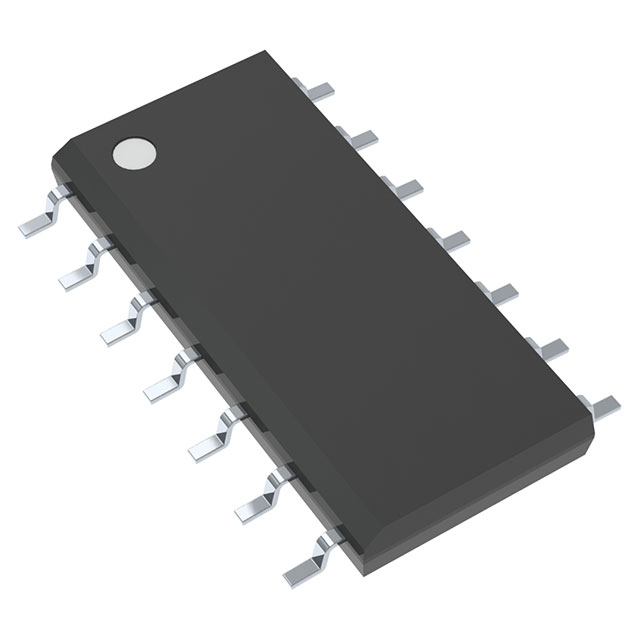
| Package / Case | 14-SOIC |
| Package / Case [x] | 0.154 in |
| Package / Case [y] | 3.9 mm |
| Trigger Type | Positive Edge |
| Type | D-Type |
| Voltage - Supply [Max] | 5.5 V |
| Voltage - Supply [Min] | 4.5 V |
Pricing
Prices provided here are for design reference only. For realtime values and availability, please visit the distributors directly
| Distributor | Package | Quantity | $ | |
|---|---|---|---|---|
Description
General part information
MC74VHCT74A Series
The MC74VHCT74A is an advanced high speed CMOS D-type flip-flop fabricated with silicon gate CMOS technology. It achieves high speed operation similar to equivalent Bipolar Schottky TTL while maintaining CMOS low power dissipation.The signal level applied to the D input is transferred to Q output during the positive going transition of the Clock pulse.Reset (RD) and Set (SD) are independent of the Clock (CP) and are accomplished by setting the appropriate input Low.The internal circuit is composed of three stages, including a buffer output which provides high noise immunity and stable output. The inputs tolerate voltages up to 7V, allowing the interface of 5V systems to 3V systems.The VHCT inputs are compatible with TTL levels. This device can be usedas a level converter for interfacing 3.3V to 5.0V, because it has full 5V CMOS level output swings.The VHCT74A input structures provide protection when voltages between 0V and 5.5V are applied, regardless of the supply voltage. The output structures also provide protection when VCC=0V. These input and output structures help prevent device destruction caused by supply voltage -input/output voltage mismatch, battery backup, hot insertion, etc.
Documents
Technical documentation and resources
No documents available


