82V3285EQG8
ActiveIC PLL WAN SE STRATUM 100TQFP
Deep-Dive with AI
Search across all available documentation for this part.

82V3285EQG8
ActiveIC PLL WAN SE STRATUM 100TQFP
Deep-Dive with AI
Technical Specifications
Parameters and characteristics for this part
| Specification | 82V3285EQG8 |
|---|---|
| Differential - Input:Output [custom] | True |
| Differential - Input:Output [custom] | True |
| Frequency - Max [Max] | 622.08 MHz |
| Input | PECL, CMOS, LVDS |
| Main Purpose | Ethernet, Stratum, SONET/SDH |
| Mounting Type | Surface Mount |
| Number of Circuits | 1 |
| Operating Temperature [Max] | 85 °C |
| Operating Temperature [Min] | -40 °C |
| Output | LVDS, CMOS, PECL |
| Package / Case | 100-LQFP Exposed Pad |
| PLL | True |
| Supplier Device Package | 100-TQFP (14x14) |
| Voltage - Supply [Max] | 3.6 V |
| Voltage - Supply [Min] | 3 V |
82V3285 Series
WAN PLL
| Part | Mounting Type | Differential - Input:Output [custom] | Differential - Input:Output [custom] | Frequency - Max [Max] | Number of Circuits | Package / Case | Main Purpose | PLL | Supplier Device Package | Operating Temperature [Max] | Operating Temperature [Min] | Input | Voltage - Supply [Max] | Voltage - Supply [Min] | Output |
|---|---|---|---|---|---|---|---|---|---|---|---|---|---|---|---|
Renesas Electronics Corporation | Surface Mount | 622.08 MHz | 1 | 100-LQFP Exposed Pad | Ethernet SONET/SDH Stratum | 100-TQFP (14x14) | 85 °C | -40 °C | CMOS LVDS PECL | 3.6 V | 3 V | CMOS LVDS PECL |
Pricing
Prices provided here are for design reference only. For realtime values and availability, please visit the distributors directly
| Distributor | Package | Quantity | $ | |
|---|---|---|---|---|
| Digikey | Tape & Reel (TR) | 750 | $ 95.44 | |
Description
General part information
82V3285 Series
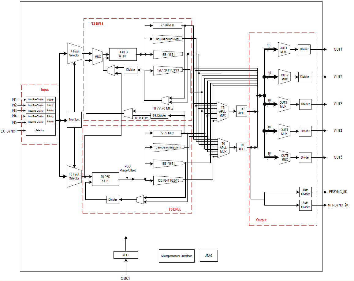
The 82V3285 is an integrated, single-chip solution for the Synchronous Equipment Timing Source for Stratum 2, 3E, 3, SMC, 4E and 4 clocks in SONET / SDH equipments, DWDM and Wireless base station, such as GSM, 3G, DSL concentrator, Router and Access Network applications. The device supports three types of input clock sources: recovered clock from STM-N or OC-n, PDH network synchronization timing and external synchronization reference timing. Based on ITU-T G.783 and Telcordia GR-253-CORE, the device consists of T0 and T4 paths. The T0 path is a high quality and highly configurable path to provide system clock for node timing synchronization within a SONET / SDH network. The T4 path is simpler and less configurable for equipment synchronization. The T4 path locks independently from the T0 path or locks to the T0 path. An input clock is automatically or manually selected for T0 and T4 each for DPLL locking. Both the T0 and T4 paths support three primary operating modes: Free-Run, Locked and Holdover. In Free-Run mode, the DPLL refers to the master clock. In Locked mode, the DPLL locks to the selected input clock. In Holdover mode, the DPLL resorts to the frequency data acquired in Locked mode. Whatever the operating mode is, the DPLL gives a stable performance without being affected by operating conditions or silicon process variations. If the DPLL outputs are processed by T0/T4 APLL, the outputs of the device will be in a better jitter/wander performance. The device provides programmable DPLL bandwidths: 0.5 mHz to 560 Hz in 19 steps and damping factors: 1.2 to 20 in 5 steps. Different settings cover all SONET / SDH clock synchronization requirements. A high stable input is required for the master clock in different applications. The master clock is used as a reference clock for all the internal circuits in the device. It can be calibrated within ±741 ppm. All the read/write registers are accessed through a microprocessor interface. The device supports five microprocessor interface modes: EPROM, Multiplexed, Intel, Motorola and Serial. In general, the device can be used in Master/Slave application. In this application, two devices should be used together to enable system protection against single chip failure.
Documents
Technical documentation and resources


